Design Guidelines for Your Next Wireless PCB
As a child, I used to watch Star Trek and always marveled at all the technology. Anything wireless on the show was particularly fascinating, especially to a 5-year old. As I aged, and as so many cool things from science fiction became reality, I realized that all these capabilities start with great PCB design.
Whether you’re building a better Wifi router, GPS system, or two-way radio, you’ll need to decide which type of antenna to use and how to connect the antenna to your PCB. If you’re working with a device that processes a large amount of data, your PCB will have to operate at high speed. Here are some design guidelines to consider when placing an antenna on your next wireless PCB.
Ground Planes Near Your Antenna
Whether you’re designing a trace antenna to print directly on your board, or if you’re planning to place a pre-packaged antenna module, placing your power and ground planes should take important consideration. You ground plane must occupy the area under your signal traces in order to provide a return path with the smallest loop area, as this will decrease EMI susceptibility.
If you’ve never placed an antenna on your PCB, your first instinct is probably to run the ground plane beneath the antenna. The antenna carries some signal, and that signal requires a return path, so shouldn’t a ground plane should sit beneath the antenna? This is not always required or advisable when working with antennas.
The whole point of an antenna is to radiate or receive radiation from an external antenna. As a solid conductor, a ground or power plane can also block about half of the emission pattern from the antenna due to reflection and absorption. This works fine with a directional transmitting antenna. With an omnidirectional antenna above a ground plane, half of the radiation pattern can be blocked by the grounding plane.
With an omnidirectional antenna, the ground plane can run right up to the edge of the antenna, ensuring that the antenna can still have nearly isotropic radiation without being blocked by any large conductive plane. This also ensures that signal traces connecting to the antenna will still have a short return to ground. Some designers prefer that the axis of your antenna run perpendicular to the edge of the ground plane, and a good portion of the radiation pattern will not intersect the ground plane.
With a ground plane antenna, the ground plane actually forms the half of the dipole antenna and must run underneath the radiating element. The conductor is connected to a signal line, and an “image” of the conductor is induced in the ground plane. Radiation is actually emitted from the ground plane in this configuration, and the conductor and ground plane form a dipole antenna. This is the configuration used in embedded and external patch antennas.
One alternative solution that doesn’t place the same ground plane constraints is to use a prepackaged antenna that connects directly to your PCB, like a rubber ducky antenna. The axis of this antenna stands perpendicular to the board, or it can also be mounted off the side of the board and connect to the board with a BNC connector.
Rubber ducky antenna on a PCB
High Gain Design
Not all devices will be designed to accommodate a larger antenna like a rubber ducky antenna due to its size. However, this type of antenna may be preferable to a ceramic chip antenna or a copper antenna printed directly on a PCB, depending on your application. Some applications will require a custom-printed antenna rather than a ceramic chip. In this case, you will want to consider some design parameters to maximize the gain of your antenna.
Antenna gain is proportional to the signal transmittance at the antenna input terminals, the conduction efficiency, and the dielectric efficiency. The signal transmittance can be easily set to 1 (i.e., reflection coefficient of 0) by impedance matching. Compensating for low conduction efficiency and dielectric efficiency requires choosing the right conductor and board material. Both parameters are difficult to calculate, but they can be determined from experiment.
Conduction efficiency is determined by the finite conductivity of the conductor in an antenna. Lower conductivity equates to lower efficiency due to IR loss in the antenna. Thus, copper is the best choice of conductor for an embedded antenna. In a PCB, dielectric losses can be reduced by selecting the right board material. FR-4 with a high speed laminate or building your board on a ceramic substrate can improve the dielectric efficiency.
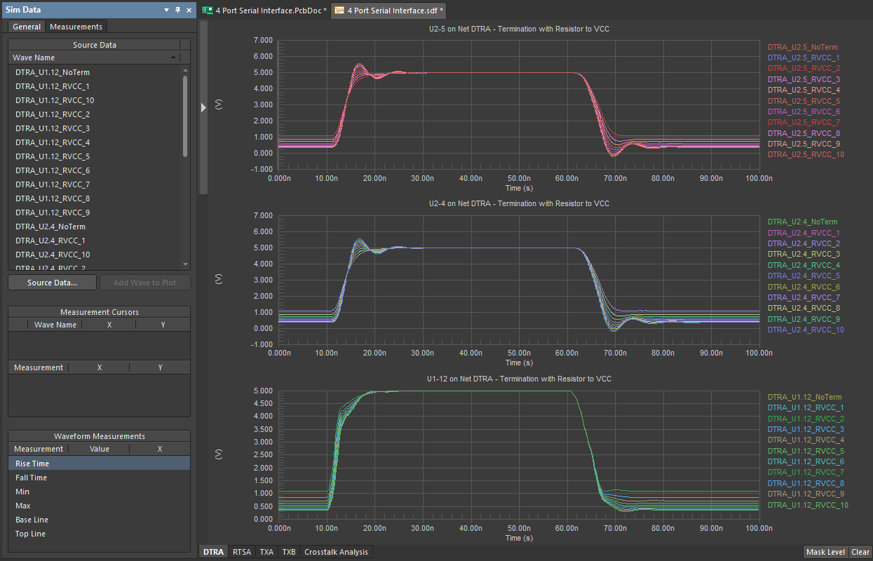
More and more electronic devices with wireless capabilities are becoming high speed/high frequency mixed signal devices. Therefore, the antenna, as well as other critical traces that behave as transmission lines, should be impedance matched to maximize efficiency.
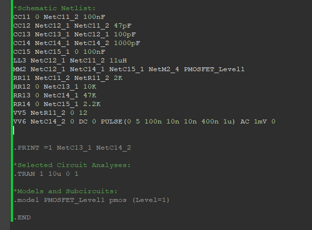
All antennas have some specified impedance at their operating frequency. Higher speed signaling between the antenna module and the rest of the components in a PCB require that everything is impedance matched. Impedance matching with an antenna can be done using a simple RC or LC circuit. However, the best choice for impedance matching is to determine the right placement of an inductor and capacitor as shunt and series elements with a Smith chart.
Utilize the proper placement tools to make your circuit board sing
With so many antenna options to consider during design, you’ll need PCB design software that includes integrated component libraries that give you all the options you need. You’ll also need signal integrity analysis tools that help you ensure your device will operate as designed. A great PCB design package like Altium Designer® has all of these tools and more.
If you’re interested in learning more about Altium Designer’s layout, simulation, and analysis features, then download your free trial. Talk to an expert at Altium today.


