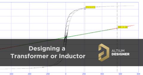
Ferrite Core Selection and Design Decisions When designing a transformer or using a ferrite core inductor, you must use the correct design process, and there is no substitution for real-world final testing. Let’s look at the process. Read Article Schematic Design Review Checklist This article is a simple, no-frills checklist to help you check schematics. Read now and avoid schematic design mistakes that could make their way into prototypes or production without a second thought. Read Article Beginner's Guide to H-bridge Full Wave Rectifier Design Need to start a new power conversion design? You’ll probably need an H-bridge full-wave rectifier to produce a stable DC output. Read Article Energy Harvesting Sensors for Medical Devices and Remote Sensors Harvesting energy from the environment is an increasingly popular technique for powering electrical devices. Let’s discuss sources and implementation. Read Article How Important is Your Microcontroller Clock Source? The type of clock signal you need to use for your microcontroller will depend mainly on the nature of the device it’s embedded in and its operating environment. Read Article MMw and RF Interaction John will generously share with us today a glimpse of his recent keynote presentation at PCB West 2021. Watch now, and don't miss this rare opportunity to learn from expert John Coonrod. Read Article Copper Pour and Via Stitching: Do You Need Them in a PCB Layout? When is it appropriate to use copper pour or via stitching in your PCB layout? Read our guide on copper pour and how it can be used properly with via stitching. Read Article PCB Design Review Checklist It’s essential to check a board for issues before production or prototyping. Here’s an extensive checklist you can adapt or use directly for PCB design review. Read Article Do You Always Need 1 oz. Copper Thickness on Each Layer? 1 oz. copper thickness is often seen as a standard thickness value used in many designs. Here’s when you might need thicker copper on every layer. Read Article Getting Started With ESP8266 A project overview on getting started with the ESP8266 device. Expert Ari Mahpour reviews the benefits of using a device such as the NodeMCU board from HiLetgo and how to get up and running with a few examples. Read Article Getting Started with MQTT and Arduino Uno Check this out. This is a new project overview demonstrating MQTT by expert Ari Mahpour. In this article, Ari answers the What and Why of MQTT, and gives guidelines to get your project started. Read Article SAP (Semi-additive PCB process): The Basics Expert Tara Dunn answers what are semi-additive PCB fabrication processes and what are the benefits? Read now and learn more about SAP. Read Article Can You Route Digital Signals on a 2-layer PCB Design? 2-layer PCBs are a common entry-level choice for designers, and they can even support high speed designs if built correctly. Read Article Deterministic Solutions to Solve Skew Problems Avoid getting your design "skewed"! Today's guest is Z-Zero's Founder and CEO, Bill Hargin. Together we will dive into the cause of getting skews in your board. Watch now to get answers to your "skews" questions. Read Article Two 4 Layer PCB Stackups With 50 Ohms Impedance Need a 4-layer PCB stackup that can support high speed components on both sides of the board? Consider these alternatives to the typical 4-layer stackup. Read Article Design to Manufacturing with a Single Mouse Click Imagine if you could design your circuit board, run simulations, source your parts, generate an accurate BOM, generate your output files and simply press a “send to manufacturing” button all within your design environment? While that may sound like a far-off dream, this interview with Misha Govshteyn from MacroFab will give you insight into how they are partnering with Altium to make this dream a reality very soon. Judy Warner: Misha, please Read Article Microstrip PCB Ground Clearance Part 2: How Clearance Affects Losses In a previous article, I provided a discussion and some simulation results on the necessary clearance between impedance controlled traces and nearby grounded copper pour. What we found was that, once the spacing between the pour and the trace becomes too small, the trace becomes an impedance-controlled coplanar waveguide (with or without ground). We also saw that the 3W rule for the spacing between the trace and the grounded copper pour is a bit Read Article Pagination First page « First Previous page ‹‹ Page37 Current page38 Page39 Page40 Page41 Page42 Next page ›› Last page Last » Load More