


Can You Route Digital Signals on a 2-layer PCB Design?

At a Glance
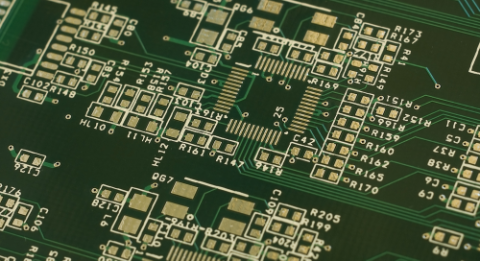
2-layer PCBs are a common entry-level choice for designers, and they can even support high speed designs if built correctly.


2-layer PCBs are a hobbyist’s best friend. They are easy to define in your design software and routing is simple if the net count is low enough. While I don’t normally work on stuff that can be done on only 2 layers, it’s still important to know how to use these boards properly. If you’re clever, you can even use these boards to route some high speed interfaces.
In this article, I want to look at some of the important rules for designing a 2-layer PCB that will use a high speed serial interface. Something like USB or SPI can be easily done on a 2-layer circuit board as long as some basic routing rules are followed. What I’ll present below should be a starting point for routing digital signals in a 2-layer PCB layout.
One point to note: you shouldn’t go into a 2-layer project like this with the expectation that this board will pass EMC testing. Ensuring EMC will depend on many factors that relate to power, grounding, your enclosure, what components and circuits are on the board, and many other factors. Hopefully, this will give you a good introduction into how you can accomplish the layout routing portion of a 2-layer PCB without creating signal integrity problems.
Getting Started With 2-Layer Digital Boards
2-layer PCB layouts are interesting as they are usually the entry level for most designers. Most designs involving a moderate-speed MCU (maybe 5-10 ns rise time), a common serial bus like SPI, and simpler high speed digital interfaces can function just fine on a 2-layer board as long as they aren’t too dense and you don’t break some basic routing rules. However, these designs often break a lot of signal integrity rules and create/receive excessive EMI. As a result, the board might technically function as you intended, but it might never pass EMC testing, so you wouldn’t be able to sell it.
First things first, there are some points to think about in a 2-layer board design that uses digital signals:
- Impedance control: Do any of your interfaces require impedance control? If so, just remember that it can be tough to hit an impedance requirements on a standard PCB thickness for single-ended signals.
- Trace length: Because we can’t hit impedance control requirements on a 2-layer board, we’ll have to keep the trace lengths below some critical length. Some interfaces are very forgiving with impedance and have long critical lengths, but you’ll need to calculate a length limit.
- Access to ground: In order to ensure low crosstalk and low EMI in your digital routing, you’ll need to provide access to ground with a clear return path.
- Part/net count: On a 2-layer board, you have limited space for routing, so you can’t have too many parts. As soon as you try to include too many parts and there is a lot of crossover in your routing, you’ll have to go to a 4-layer board, or you’ll have to make your 2-layer board too large.
Digital Signals and Impedance
In working with digital logic, especially in a 2-layer board, it’s important to note that not all digital signals have an impedance requirement. Sometimes, if they do, you can violate it and the interface will work fine. This is important in a 2-layer board because, if you just want to route microstrips, the width of your traces needs to have a specific value to hit an impedance target.
Typically, the impedance target you see for digital signals will be as follows:
- Some single-ended impedance requirement, where the signal is taken in isolation
- Some differential impedance requirement for differential pairs, where the signals must be routed together
Just as an example, consider a 2-layer board on standard thickness 62 mil core (Dk = 4.8). If we want to hit the standard 50 Ohms impedance target, then we need to have a trace width of almost 110 mils! This is a huge trace width and is much larger than the pad size of any digital component you’ll place on a real board. To determine this, I used an online microstrip impedance calculator based on the IPC 2141 formulas.

Online calculators don’t give the most accurate results, but the above result illustrates an important point: you can’t possibly do impedance control for isolated single-ended traces on a 2-layer PCB and expect to fit everything in the layout. Obviously, this would eliminate the use of DDR for memories, which includes single-ended traces with high speed signals and very small electrical lengths.
This is where we need to set a length limit on your traces if we’re using a controlled impedance interface. When the distance traveled by the signal during its rise time is much longer than the length of the trace, then the impedance of the trace doesn’t matter. In this case, the signal only sees the load’s impedance during propagation. The exact length limit depends on multiple factors, but a very conservative rule is to set a trace length limit of 1/10th the distance traveled by the signal.
Just as an example, let’s use the propagation delay in the above image with a 5 ns rise time signal. In the above case, the propagation speed is about 6.8 inch/ns. So this means, if we have a 5 ns rise time signal, then the signal will travel 34 inches during its rise time, so our maximum trace length would be 1/10th of this, or 3.4 inches. We can actually be a bit less conservative than a 1/10th length limit. If we set a 1/4th length limit, we would have a maximum trace length of 8.5 inches before we need to start worrying about impedance of traces.

Depending on how much of an impedance violation you can tolerate at the receiver end of your channel, you will definitely have some freedom to implement a 2-layer board with a typical digital protocol as long as lengths are short.
What About Differential Impedance?
As I’m sure readers will be aware, most high speed interfaces care about the differential impedance, not just the single-ended impedance. As we saw above, a single-ended trace would need to be unacceptably large in order to hit a 50 Ohm impedance value you’ll see in most specs. How can we hit a differential impedance value on a 2-layer board when the characteristic impedance trace width requirement is so big?
Some interfaces can actually be routed as length-matched single-ended traces, or as tightly coupled differential pairs! USB is a perfect example: the termination scheme treats each end of the pair individually as a single-ended trace, so we still have to hit the single-ended impedance spec. How can we possibly do this?
In this case, we need to leverage a calculator to get the differential impedance and use that returned width and clearance value to ensure we’ve hit the single-ended spec. In a 2-layer board, we can’t just take the width we found above and plug it into a differential impedance calculator. If we did, we’d find that the required trace separation was about 10 inches! Obviously, this isn’t practical. In reality, if we calculate the trace width and spacing we need for a target impedance, we’d have something closer to 10 mils width and 6 mils spacing for a coplanar microstrip arrangement. This is much more reasonable.
What this means is:
- The trace width needed in a differential pair does not have to be equal to the trace width needed to hit the characteristic impedance for a single trace. In a differential pair, the single-ended trace width defines the odd-mode impedance, which is half your differential impedance target. The odd-mode impedance value is different from the characteristic impedance value.
This is an important distinction. It means that, for a differential interface, you shouldn't just take the trace width for the characteristic impedance shown above and just plug it into your differential impedance calculator to get a spacing. When the traces in a differential pair are brought close together, the coupling between them reduces the single-ended signal impedance and causes the required trace width to be smaller, even on a 2-layer PCB. We’ll discuss this more in two upcoming articles on this topic, including an example where we look at using USB on a 2-layer board.
Some 2-Layer Routing Guidelines for Digital Signals
The goal of these basic guidelines is to ensure your digital design has the lowest noise possible, which is difficult given the structure of a 2-layer board.
- Place a ground plane on the bottom layer, and then place digital components and routing on the top layer. This won’t help you with impedance control while routing, but you should do this anyway to help with noise control and to give you easy access to ground through vias.
- Use a fixed trace width for routing power and signals. 8-10 mil traces are just fine for routing digital signals, and 12-14 mil vias are fine for signal transitions back to the ground plane. Power could be routed with polygons if you’re working with high current, but in most cases you’ll be fine with wder traces.
- Use decoupling/bypass capacitors to ensure stable power and low ground bounce. 2-layer boards can exhibit ground bounce and possibly some noise on the power rails, but decoupling/bypass capacitors will damp this noise.
In the next installment in our 2-layer board series, I’ll show how to implement these design guidelines for USB, which can definitely be counted as a high speed digital interface. If you’re familiar with USB, you’ll know that it’s a fast interface that often needs impedance controlled routing. However, with the guidelines shown above, you can get to a functional 2-layer board that uses this interface. Just note that you might not have a totally noise-free board, so don’t expect this layout to automatically pass EMC testing. However, it should work fine as a development board for your favorite microcontroller, and you might get lucky if you route your signals correctly with a consistent ground plane on the back layer and you limit layer changes through vias.
When you need to design a 2-layer board that can support digital signals, use the PCB design tools in CircuitMaker. All CircuitMaker users can create schematics, PCB layouts, and manufacturing documentation needed to move a design from idea to production. Users also have access to a personal workspace on the Altium 365 platform, where they can upload and store design data in the cloud, and easily view projects via a web browser in a secure platform.
Start using CircuitMaker today and stay tuned for the new CircuitMaker Pro from Altium.

About Author
Related Resources
Related Technical Documentation
Table of Contents
Design to Release, Without the Friction
- Keep reviews tied to the right version
- Reduce handoff confusion and rework
- Spot sourcing and release risk earlier
- Work solo, share when needed
Get Started
Thank you, you are now subscribed to updates.