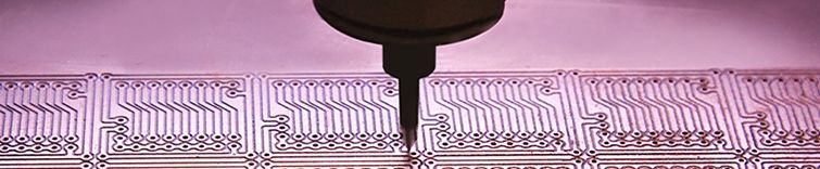
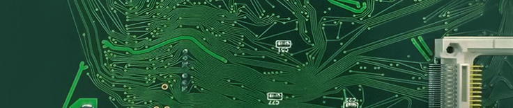
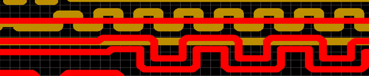
Mobile menu
PCB Design
Altium Designer
World’s Most Popular PCB Design Software
CircuitStudio
Entry Level, Professional PCB Design Tool
CircuitMaker
Free PCB design for makers, open source and non-profits
Why Switch to Altium
See why and how to switch to Altium from other PCB design tools
Solutions
For Enterprise
The Last Mile of Digital Transformation
For Parts and Data
Extensive, Easy-to-Use Search Engine for Electronic Parts
Altium 365
Resources & Support
Explore Products
Free Trials
Downloads
Extensions
Resources & Support
Renesas / Altium CEO Letter To Customers
All Resources
Support Center
Documentation
Webinars
Altium Community
Forum
Bug Crunch
Ideas
Training & Education
Professional Training
Courses & Certificates
Training Previews
On-Demand
Instructor-Led Trainings
Education
Programs
Educator Center
Student Lab
Altium Education Curriculum
Store
Search Open
Search
Search Close
Sign In
고속 설계
Main Korean menu
블로그 홈
PCB 디자인
팀 공동 작업
설계 데이터 관리
ECAD/MCAD
고속 디자인
PCB 라우팅
공급망
전력 무결성
리지드 플렉스
회로도 캡처
신호 무결성
시뮬레이션 / 분석
응용프로그램
알티 움 (365)
알티 움 디자이너
리소스
엔지니어링 뉴스
가이드 북
팟 캐스트
웹 세미나
하얀 종이
고속 PCB 설계
고속 설계 문제에 대한 간단한 솔루션
솔루션 살펴보기
고속 PCB 설계
Overview
All Content
Live Webinars
Filter
0 Selected
Clear
×
Clear
Whitepapers
적층 구조를 올바르게 설정하기
PCB 설계에서 부적절한 레이어 스택은 제작 실패와 거부로 이어지는 가장 흔한 오류 중 하나입니다. 모든 멀티레이어 회로 기판은 PCB 제조로
Pagination
First page
« First
Previous page
‹‹
Page
14
Page
15
Page
16
Page
17
Page
18
현재 페이지
19
💬
🙌
Need Help?
×
📞
1-800-544-4186
📞
1-858-864-1798
✉️
sales.na@altium.com
🛟
Support Center
🎓
Training Support
📣
Ask Community
📞
Contact Us