Skip to main content
Mobile menu
Discover
Develop
Agile
Resources & Support
Free Altium 365 Tools
Gerber Compare
Online PCB Viewer
Resources & Support
Learning Hub
Support Center
Documentation
Webinars
Altium Community
Forum
Bug Crunch
Ideas
Education
Student Lab
Educator Center
Altium Education Curriculum
Search Open
Search
Search Close
Sign In
Main menu
Home
PCB Design
Collaboration
Component Creation
Data Management
Design Outputs
ECAD/MCAD
HDI Design
High Speed Design
Multi-Board
PCB Layout
PCB Routing
PCB Supply Chain
Power Integrity
RF Design
Rigid Flex
Schematic Capture
Signal Integrity
Simulation
Software
Develop
Discover
Agile
Altium 365
Altium Designer
Education
Programs
Altium Academy
Engineering News
Guide Books
Newsletters
Podcasts
Projects
Training Courses
Webinars
Whitepapers
Top 4 Time Wasters in PCB Design Collaboration
An essential aspect of project management is time management, especially when your design team is working remotely. Your time management strategy is team-based and individual, but time can easily get spent on important tasks when working as part of a team. So, how can you streamline important collaboration tasks for your design team to increase productivity? The first step is realizing where time is being wasted during design, followed by finding
Read Article
DOE Releases Roadmap for Quantum Networking and Quantum Internet
Now with quantum computing going mainstream, quantum networking is on the horizon. Here’s how this differs from classical networking.
Read Article
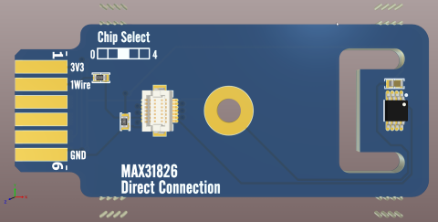
Temperature Sensor Project: Digital Temperature Sensor ICs
The final article in this series looks at digital temperature sensors pitting all the sensors we’ve tested against each other in a head to head contest over a wide range of environmental conditions to allow for a comparison of their functionality, accuracy, and behavior.
Read Article
Transmission Line Transfer Function from ABCD and S-parameters
High frequency and data rate channels can be routed as a mode-selective transmission line. Here’s when you should consider this routing technique.
Read Article
How to Involve Customers in PCB Product Development
If you’re a freelancer and you’ve led or managed a complex PCB design project, the need to involve your customer in the product development process may not be obvious. Your customer is probably a project manager at a bigger company, so they’ll be overseeing progress on the project and leading communication with you. If you work on a small team or as part of a large organization, involving customers in product development can be time-consuming
Read Article
The Advantages of ABCD Parameters for Analyzing Your PCB
SI (Signal integrity) engineers always talk about S-parameters, but an alternative tool for circuit design and analysis is ABCD parameters.
Read Article
EMI Filter for Simulating Noise Suppression with Altium Designer 20 and Altium 365
Simulations can get very complicated, but Altium 365 helps you keep your simulation models and data organized.
Read Article
Backdrilling in PCB Design: An Easy Way to Improve Via Signal Integrity
Backdrilling in Altium Designer is one of the easiest ways to improve via signal integrity. Read on to learn about back drilled vias and more.
Read Article
Stripline vs. Microstrip Trace Width for Desired Impedance: Are They the Same?
Stripline vs. microstrip width values are quite different; they can’t simply be interchanged. Let’s break down why and what you can expect from your PCBs.
Read Article
Data Rate vs Bandwidth: What's the Difference?
What is the difference between data rate vs bandwidth? This topic has been obfuscated for the last 30 years. Here’s how they relate.
Read Article
Pagination
First page
« First
Previous page
‹ Previous
…
Page
165
Page
166
Page
167
Page
168
Current page
169
Page
170
Page
171
Page
172
Page
173
…
Page
180
Page
190
Page
200
Page
210
Page
220
Page
230
Page
240
Page
250
Page
260
Page
270
Page
370
Next page
Next ›
Last page
Last »
Subscribe to