


3D-MID Design Guide: A Comprehensive Whitepaper

At a Glance
Discover how 3D-MID technology integrates circuits into 3D structures. Download the whitepaper to explore design, applications, and Altium capabilities!


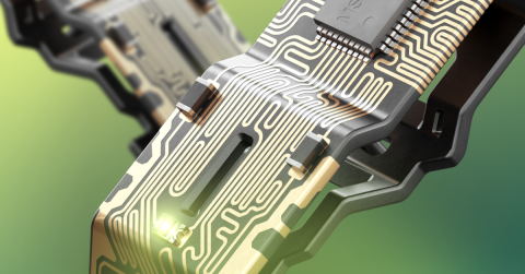
A mechatronic integrated device (MID) is an injection molded plastic which incorporates a conductive circuit pattern and integrates both mechanical and electrical functions. It’s the fusion between a plastic part and a circuit.
Copper traces are etched onto the surface of the plastic part, creating tracks and pads that can then house electrical components. What you get is a cool electromechanical piece of hardware.
These innovative devices offer a unique solution to the challenges of modern design, providing a platform for integrating electronic circuitry directly into three-dimensional structures. Supporting this innovative technology is Altium. Altium 3D-MID design tool offers support for 3D layout, routing, and design rules.
Want to dive deeper into 3D-MID design and its applications? Download the comprehensive whitepaper now and explore how this technology is transforming electronics design!


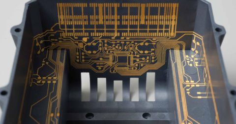
MID before after component placement
Where & Why Are MIDs Used
According to IDTechEx, the Market for 3D/additive electronics is expected to increase from about $800 Million in 2020 to around $1.3 Billion by 2030.
You can find MIDs across many industries and products, from medical to automotive industries, cell phones, and tablets. MIDs make sense for these industries and products because of the need for sleeker designs. Sometimes, it’s not practical or possible to have many interconnect components and wires. Phones are a great example of this.

We’re always trying to pack more in a smaller package, so something like a MID can help us out. By using a mechatronic integrated device in a phone, we can have the antenna integrated with the mechanical enclosure, saving us space on our board and even giving us a better-functioning antenna. These same principles can be applied to any field, including automotive. Below, you can see MID technology in a car steering wheel, eliminating the need for wire harnesses.

The medical field also benefits from MIDs in the development of advanced medical devices, enabling the miniaturization of electronic components and the creation of smaller, patient-friendly solutions.
MIDs serve as an innovative technology across various sectors, offering compact and integrated solutions that enhance performance, reduce weight, and contribute to electronic systems’ overall efficiency and reliability.

Take a look at what Harting did. By using MID technology, it was possible for Harting to develop a lighting module with a compatible interface that enables a cost reduction of 35% compared to the previous solution with a significantly lower installation height and reduced number of parts.

The Current Problem With Designing 3D-MIDs
Most MID designs are done using mechanical CAD tools, which isn’t ideal when working with electronics. This existing workflow poses several drawbacks.
- There is a lack of schematic intelligence to drive the layout
- Manual process of footprint creation
- Distortion and manual merging issues due to projecting 2D sketches on 3D surfaces
- 2D to 3D projection issues including distortion and manual merging
Using Altium to natively design these MIDs solves these issues.
Benefits MID Design in Altium
- Accurate Designs - Because you are designing directly on a 3D substrate and not projecting a 2D design onto a 3D structure, you can achieve accurate results.
- Reduced risk of issues - Apply clearance, trace width, and other design rules to your design to minimize any design issues.
- Correct Fitment - Mechanical CAD collaboration guarantees design synchronization with your electro-mechanical product.
- Precise placement - Alignment grids and visual connection lines ensure proper component placement and connectivity for your product.
- Minimized manufacturing problems - Give manufacturers exactly what they need with fully customizable design outputs.
- Unified Design Environment - Work in an electronically intelligent product where the schematic drives your layout
Summary of Altium MID Capabilities
Below, you’ll find the latest features for our 3D substrate design technology. This new feature is still under active development, which means that we will continue to improve and introduce new capabilities. Let’s take a look at some of the main features available for use today.
MCAD Integration: Sketch Projection


When designing the substrate in MCAD, 3D curves can be placed on the part’s surface and included in the exported IGES file. These “curves” can then be included in the IGES export using the Export 3D Curve features option. When the IGES file is imported into Altium to form the substrate for a 3D-MID, these elements can be displayed by selecting the View » Show Sketches command.
Alignment Tools

Within the 3D-MID document, you can effortlessly generate a grid on any of the three datum planes using the Alignment Grid section in the Properties panel. Once created, the grid is projected from the specified plane onto the surfaces of the 3D substrate. This grid operates independently of any sketches imported as part of the substrate. Users have full control over the properties of the grid, with considerations for grid snapping, visibility, and various dimensions.
Routing Customization
Just like in a standard flat design, routing can be fully customizable with routing widths, clearance rules, and other design rules. Plus, with visual connection lines and alignment grids, the placement of traces and components is precise and accurate.

Via Placement
Vias can be incorporated into the 3D-MID manufacturing process, subject to constraints. For detailed manufacturing capabilities, consult with the manufacturer. Although full via support is pending in the 3D-MID tool, you can include them manually. Treat each via pad as a component, and create a corresponding single-pin symbol and a footprint with a single pad. Manually place, assign net names, and route vias using the process described here.

Solid Region Placement
The support of the Solid Region enables the creation of various copper shapes on a 3D structure. Functionalities include snapping to alignment grids and imported sketches, as well as the ability to toggle region areas during placement.
Once placed, regions can be selected, edited for net connections, and deleted. Curved regions traced from imported sketches are recognized, and overlapping regions on the same net are merged during export, facilitating the creation of complex shapes.

Conclusion
MIDs mark a groundbreaking leap in electronic design, allowing seamless integration of circuitry into three-dimensional substrates. Altium’s advanced 3D-MID design tool positions itself at the forefront of this transformative technology.
MIDs prove their value across diverse industries, from automotive and consumer electronics to medical devices, and aerospace applications. Their direct integration into structural elements enhances system performance, reduces weight, reduces costs, and contributes to overall efficiency. mechatronic integrated devices emerge as a transformative technology, providing compact, integrated solutions that redefine electronic system design across sectors.
Incorporating MIDs into your next electronic project is a transformative choice, and for optimal design precision and efficiency, Altium stands out as the premier tool for unleashing the full potential of this cutting-edge technology.
Related Resources
Design to Release, Without the Friction
- Keep reviews tied to the right version
- Reduce handoff confusion and rework
- Spot sourcing and release risk earlier
- Work solo, share when needed
Get Started
Thank you, you are now subscribed to updates.