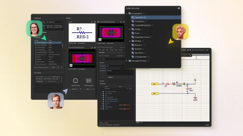


Altium Designer, in conjunction with the Altium 365 Workspace, brings support for an advanced project construct that targets the development stage of the project lifecycle, simplifying the creation and ongoing workflow for version-controlled projects. Centralized storage under the control of the Workspace also enables this feature to be a foundation for other collaborative services. Some key…
This article introduces the Draftsman board fabrication view in Altium Designer, explaining how it creates an automated drawing of a bare PCB from the top or bottom side and how that view can be configured through the Properties panel. You will see what controls are available for scale, title, line style, source layer, view side, rotation, drawing and polygon display modes, color overrides,…
This article walks you through how to read and work with signal integrity analysis results in Altium Designer, focusing on how reflection and crosstalk data are organized in the SDF document, what charts, plots, and waveforms represent, and how different termination settings and sweep options affect what you see. It also explains how to cross probe from a waveform back to the PCB after post…
This article walks you through how to configure and run a signal integrity analysis in Altium Designer, from the initial SI Setup Options through using the Signal Integrity panel to review screening results, investigate failed or unanalyzed nets, and adjust preferences. It explains what happens in schematic-only mode, how default tolerances and rules are applied, and how to use the available…
This article walks you through the setup work required before running Signal Integrity analysis in Altium Designer, so you can avoid invalid results and understand what the analyzer needs from your design. It explains which nets can actually be analyzed, why correct component and pin model assignments matter, how supply net rules and PCB layer stack settings affect the process, and how to use the…
This article explains how BOM CoDesign in Altium Designer helps ECAD and procurement teams work together by comparing a project’s live ActiveBOM with related Managed BOMs and their releases, created through the BOM Portal in your connected Altium 365 Workspace. You will see how to access related BOMs, review release details, understand detected differences, use comparison and exploration actions…
This article walks you through how to troubleshoot simulation failures in Altium Designer by helping you determine whether the issue comes from the circuit itself or from the simulation setup. It explains the difference between warnings and fatal errors, outlines why convergence problems happen in SPICE, and provides practical troubleshooting steps for Operating Point, DC Sweep, and Transient…
This article serves as a guide to advanced simulation resources in Altium Designer, helping you find the right reference whether you need to troubleshoot a failed simulation, understand simulation-ready generic components, work directly with a SPICE netlist, or create your own simulation models. It is a useful starting point for users who want to move beyond basic simulation tasks and better…
This article explains how to create, find, place, organize, edit, and manage snippets in Altium Designer using the Design Reuse panel. It covers both Workspace and local snippets, shows how snippets can capture schematic or PCB circuitry for reuse, and outlines the key actions available for maintaining them, including folder organization, revision-related details, and management options for…
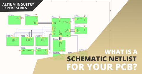
Parent page: More about Schematics Related Resources Multi-Sheet and Multi-Channel Design Compiling and Verifying the Design Design Synchronization It's the components and how they connect to each other that creates your unique, electronic circuit. In the schematic you create the logical representation of your design by connecting the component pins together, to design the printed circuit board…
Learn More