Working Through Circuit Simulation for Free Often Won’t Work, Try Altium Designer

Electronic Design Automation (EDA) software provides the tools that support the design and analysis of electronic devices, systems, and printed circuit boards. Within this broad definition of EDA software, some companies offer free PCB design programs while others focus on schematic capture, mixed-signal simulation, Very Large-Scale Integration (VLSI) circuit design, and customizable design rule checking. While many EDA software applications emphasize several aspects of PCB design, Altium Designer follows a unified design environment approach that covers the entire PCB design process.
ALTIUM DESIGNER
The best software around for analysis and simulation designing.
Altium’s attention to detail becomes apparent through the mixed-signal circuit simulation, signal integrity analysis, and power integrity analysis capabilities found within Altium Designer. Based on the enhanced version of the event-driven XSpice, the Simulator provides support for PSpice® device models and the Digital SimCode™ language. With these capabilities in place, you and your design team can test ideas and designs before committing to the prototype and manufacturing stages. In addition, circuit simulations allow design teams to measure board performance in a virtual—rather than physical--working environment.
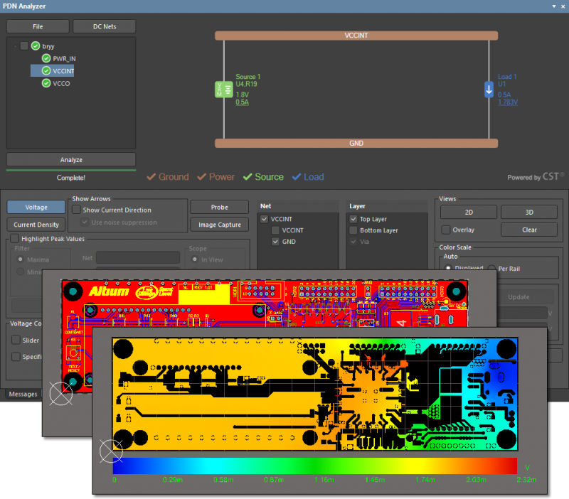
While operating differently than circuit simulators, Altium’s post-layout signal integrity analysis offers a detailed look at the behavior of circuit routing. Altium’s PDN analyzer ensures the effectiveness of the DC power delivery systems for a PCB design. The DC analysis tests the planes, traces, and vias that provide the power consumption requirements for the PCB.
Altium Designer Provides Mixed-Signal Simulation Tools
Mixed-signal simulators analyze circuits that include analog and digital devices. Altium Designer allows you to run the circuit simulations directly from the schematic by using the Mixed Sim toolbar. Prior to running a simulation, you and your team must ensure that the schematic contains components that have SIM models attached, voltage sources, a ground reference for the simulations, and net labels linked to the circuit points that will display waveforms.
When working within Altium Designer, you can find components for the schematic by accessing the Libraries tab and searching by component name or number. After locating the component, you will also need to select the simulation model for the component from either the Model Library or from the manufacturer’s website.
Another step towards building the simulation involves adding voltage sources. Altium Designer provides a Library Simulation Folder that contains voltage source dialogs. Altium eases the process of defining the values for the voltage by providing menu-driven options and by automatically creating parameters. After you have defined the voltage source values, Altium provides additional dialogs for placing the power source within the circuit.
|
Mixed-Signal Simulation Type |
Mixed-Signal Simulation Purpose |
Simulation Requirements |
|
Operating point analysis |
Determines DC Bias of Circuit |
Must run before the Transient Analysis |
|
Transient analysis |
Generates output normally shown on an oscilloscope and calculates voltage, current, or power as a function of time over a user-specified interval |
|
|
DC sweep analysis |
Performs series of operating point analyses and generates a curve trace output |
Requires primary source |
|
AC small-signal analysis |
Generates output that shows the frequency response of the circuit |
|
|
Noise analysis |
Small signal analysis performed at discrete frequencies using noise sources attached to noise-generating elements in a circuit |
|
|
Pole-zero analysis |
Studies behavior of linear, time invariant networks |
|
|
Transfer function analysis |
Calculates the DC small-signal transfer between an input |
|
|
Temperature sweep |
Runs DC or Transient analysis as the circuit temperature changes |
|
|
Parameter sweep |
The value of a device changes in increments over a specified range. Explores variations in component values without editing the circuit multiple times |
Requires enabling of AC, DC, or Transient analyses. |
|
Monte Carlo Analysis |
Statistical analysis shows how changing component properties impact circuit performance |
Performs passes on any enabled standard analysis |
Mixed-Signal Simulation Options
Build Circuit Connectivity and Establish Security in Your Designs
Altium simplifies the process of building circuit connectivity and adding power ports with an easy-to-use Wiring Tools toolbar. To view signals during the simulation, your team must place net labels at key points on the circuit. The final step of compiling the project establishes the error checking for drafting and electrical rules violations. After entering the Analysis Setup menu, you and your design team can enable a circuit simulation by selecting options from menu choices.
Within the general setup, Altium Designer also provides simulation options that allow your team to determine the type of data collected, the scope of the simulation, and the signals that the simulation will automatically display. The SimData Editor’s Waveform Analysis window shows the results of each analysis. If the simulation produces warnings or errors during the generation of the SPICE netlist, the messages display in the Messages panel. No errors in the circuit allow the Spice netlist to move to the Altium Designer simulation engine.
- Learn about SPICE simulators online
- Learn about managing net connection order throughout PCB layout
- Learn about highlighting nets within Altium Designer
Use Altium’s Advanced Design Technologies for Signal Integrity Analysis
Many EDA software packages lack the capabilities needed to support high speed, multilayer designs. Altium Designer builds on its unified design environment with pre-layout and post-layout signal integrity analysis. The signal integrity simulator that models the behavior and interaction of circuit transmission lines through the use of algorithms.
By running the signal integrity analysis from source schematics prior to the PCB layout and routing, you can check for mismatched net impedances. Because of the signal integrity screening functions as part of the Altium Designer’s design rules system, you can use the Design Rule Checking system to check for signal integrity violations. As a result, you can check for signal reflection, overshoot, undershoot, and crosstalk. Altium Designer includes the functionality of showing available termination options for solving signal integrity problems.
Succeed Together with Unified Design Teams
Your design team can view the results of the signal integrity analysis at the Signal Integrity panel. With a “passed” having the values within the limits defined by the tests, the panel also shows nets that passed the different signal integrity tests. Highlighted in red by the panel display, failed nets have at least one value outside the criteria defined by the tests.
- Learn more about avoiding signal integrity loss in your designs
- Learn more about analog or digital converters and how they affect signal performance
- Learn more about high-speed design analysis with simulation and signal integrity checking

Any board should be thoroughly checked before being put through to manufacturing
Ensure the Effectiveness of Your DC Power System with Altium’s PDN Analyzer
High-speed, multilayer circuits push DC power systems to the limit. To ensure that those systems provide the optimal performance needed by your PCB design, Altium uses the PDN Analyzer to establish the DC analysis of the Power Delivery Network (PDN) and to test the DC power integrity (PI-DC). As part of the PDN Analyzer, the DC Power Integrity simulation tool benchmarks the DC performance of a PCB against electrical and physical properties. For example, the PI-DC analysis checks power and ground plane shapes for proper sizing while also studying the voltage drops and current densities of the PDN.
Circuit Simulation Ought to Come with Your Design Tools
Available as a downloadable extension for Altium Designer, the PDN Analyzer works as part of the unified design environment. As a result, the PDN Analyzer operates within Altium Designer by starting from the Schematic Editor or the PCB Editor. Altium Designer provides the results through 2D/3D modeling of the PCB copper layout. With this approach, the PDN Analyzer visually models the power source and automatically pulls all physical and electrical information from the PCB design.
- Learn more about Altium Designer's high-speed design capabilities
- Learn more about Altium Designer's native 3D design engine
- Learn more about Altium Designer's brilliant unified design environment approach

PDNA is vital to the survival of your board
The unified design environment offered through Altium Designer allows you and your team to manage and test your PCB design without moving from one EDA application to another. Altium Designer provides a comprehensive suite of analysis tools that cover circuit performance, signal integrity, and DC power systems.


