PCB Simulation: How to Simulate a PCB Design

Every PCB needs to go through some level of evaluation before it can be placed into high-volume production. Designs will generally go through electrical testing during fabrication and assembly, but there are some specialized areas of mechanical and electrical behavior that are difficult to quantify during a test once the board is assembled. Instead of testing every aspect of a design, electrical circuit design simulation software can be used to calculate electrical behavior in your PCB board simulator before production.
Why use PCB design simulation tools instead of testing everything? It is often the case that some electrical characteristics are difficult to test without building specialized test boards and fixtures or without using some kind of circuit tester program. Some aspects of a design are simply too expensive for some designers to test. For example, the instruments required to comprehensively measure signal behavior in a high-speed transmission line can cost $250,000 or more. PCB design simulation tools allow designers to calculate the same signal behavior they might need to measure in a design, and often in a realistic setting with data directly from the PCB layout. In this overview, we'll look at some of the important points involved in building and running Altium PCB simulation software, both inside your PCB design and circuit simulator software and in external applications.
- Front-End Simulation and Evaluation
- Impedance Calculations in PCB Stackup Design
- Simulations During PCB Layout and Routing
- Post-Layout Simulations
- More Advanced PCB Simulations
Front-End PCB Simulation and Analysis
PCB simulations begin in the schematic capture phase of a design project, where SPICE simulations are used as part of circuit design. SPICE simulations are important for evaluating system-level electrical behavior, but they are also useful for circuit optimization as part of the design process. Schematic capture software with a built-in SPICE simulation package can help you stay productive while you work through some of the basic simulations needed to evaluate electrical behavior.
SPICE packages that are used for front-end engineering and simulations are designed to perform a specific set of analyses:
- DC sweeps, where input DC voltage is swept through a series of values and the voltage and current at other nodes are monitored
- Transient analysis, or time-domain mixed-signal simulations, is the fundamental time-domain simulation
- AC sweeps, or frequency sweeps, where the frequency of an AC signal is varied in time
- Parameter sweep, where a specific set of component parameters is swept across a range of values
- Pole-zero analysis, where stability conditions and transient oscillation frequencies can be visualized in a single graph
Some schematic capture programs with integrated SPICE engines can be used with more advanced simulations, such as noise analysis and thermal analysis.
Most designers are probably familiar with using SPICE for analyzing basic linear or nonlinear circuits, but they can also be used to examine real components as long as a SPICE subcircuit model is available for the component. SPICE models can be custom-written for components based on their input-output relationships and logical conditions at the component inputs. These models might be provided by component manufacturers so that a designer can properly simulate a component's behavior alongside other circuit elements.
SPICE simulations can be used at multiple stages in the design process to qualify electrical behavior in important circuits. After a SPICE simulation is set up, it can be run multiple times in different stages of the design process. Once a SPICE simulation is completed, the data can be displayed in graphs for further examination and analysis. Electrical behavior that might lead to signal integrity problems can often be identified at this stage, offering a chance to modify a design before proceeding to the PCB layout.

While SPICE is most common for front-end simulations during schematic capture, other front-end tools in electrical circuit design simulation software like IBIS models and Multisim models can be used to simulate electrical circuits, components, and even entire systems. After an initial design is completed and evaluated, it can be transferred into a new PCB layout and evaluated further.
Impedance Calculations in PCB Stackup Design
Once the initial set of schematics has been created, simulated, and evaluated, it's time to create a stack-up for the bare board and determine impedance. The impedance of high-speed nets in your PCB stack-up needs to be accurately determined, often with an accuracy of greater than 95%. The goal here is to take your proposed stack up and use it to determine the trace width that is needed to ensure an interconnect has a required target impedance. Although there are formulas that can be used to size traces with the required width, these formulas might be inaccurate, and a more sophisticated simulation would be needed to determine the impedance of single-ended traces and differential pairs on different signal layers.
Advanced PCB stack-up calculators will use the boundary element method, moment of methods, or finite element method to determine the impedance of a trace at specific frequencies. These numerical calculations automate the process of determining the trace width required for a specific impedance; most calculators force you to use an outdated formula from IPC-2141, or they require you to manually iterate through trace width values until you happen to hit your target impedance value.

There are some important parameters that your stack-up editor needs to use to determine impedance at high frequencies:
- Copper roughness: This parameter is specific to the manufacturing process, and it will effectively increase the skin effect impedance in a trace.
- Dielectric dispersion: This parameter tells you how the speed of light and losses vary in the PCB substrate.
The best PCB impedance calculator utilities inside PCB design simulation tools will include these effects so that impedance can be determined with very high accuracy. Once the trace width required for specific nets to have a target impedance (usually 50 Ohms) is determined, it can be set as a design rule in your PCB routing utilities.
Simulations During PCB Layout and Routing
Once a component placement is finalized and a design is ready to be routed, signal integrity problems can creep in if a design is not evaluated during the layout phase in any circuit tester program. Although you might obey best routing practices, it's still possible a placement decision or routing decision induces some signal integrity problem that was unanticipated. These potential problems need to be identified and corrected during the routing phase rather than when the design is completed. Waiting until the design is finished to run signal integrity simulations creates a risk that large amounts of re-routing need to be performed, but this can be avoided with some simple design rule-based simulations in the PCB layout.
The best PCB layout and routing software will include a signal integrity engine that allows you to inspect overshoot and undershoot in your signals as you route them, rather than using a more advanced field solver at the end of a design. This is important as many aspects of a real layout that can influence signal behavior, namely parasitics and lack of termination, can't be quantified in a SPICE simulation. The best routing design simulation tools allow you to define signal integrity requirements as part of your routing tools, and your design software can automatically check conformance as you create your PCB board simulator layout.
To start this kind of simulation during routing, there needs to be a model for the driver and receiver buffers in the components used in the PCB. There are generally three options:
- Use a circuit model to create an equivalent circuit for the receiver's input buffer
- Use IBIS models to represent I/Os on driver and receiver components
- Use a model representing a standard logic family
The first two options involve significant effort in front-end schematic capture in order to define buffer models and set them for each I/O on a component. For many integrated circuits, these IBIS or circuit models do not exist and the model parameters must be determined from S-parameter measurements. Once a buffer model or an appropriate logic family model is selected for the I/Os on a component, signal integrity simulations can be performed on the connected nets to better understand signal behavior.

Once model settings are applied in schematics, it is possible to experiment with signal integrity simulations while routing. This can be done directly from a PCB layout, but before the rest of the layout is finished. If this is done mid-layout, it should only be done on the nets that are most susceptible to signal integrity problems. Examples include very fast edge rate differential nets and push-pull single-ended I/Os in parallel buses, the latter of which may not have an impedance specification.
Some of the other important simulation metrics to examine in an electrical circuit design simulation during the layout phase are reflections and crosstalk. Both of these can be evaluated with a lightweight 2D solver inside a PCB editor, and the results can be visualized on a graph in the time domain. These features are excellent for quickly identifying interference on critical nets (crosstalk simulations) or quickly determining the need for the termination in an interconnect. One important feature from SPICE that also appears in PCB layout simulations is the ability to use a parameter sweep to iterate through possible termination values. These results can be displayed on a series of overlaid curves for comparison.

After cleaning up a design and ensuring signal behavior meets performance metrics, post-layout simulations should be performed to identify system-level design defects in the PCB layout.
Post-Layout Simulations
Once the PCB layout is completed, it's time to qualify the design again using post-layout simulations. These simulations are run inside the finished PCB layout to ensure the completed design matches the original evaluation metrics. This can be as simple as re-running the previous set of simulations used in layout and routing, while additional simulations can be used to quantify potential thermal and DC power problems. There are other post-layout simulations that may be needed to fully evaluate a design, but these can be addressed with field solver applications (see below).
Some of the important metrics to evaluate in post-layout are signal integrity metrics, which are encoded in your design rules and routing tools if you're using the right PCB design and circuit simulator software. As part of a final design rule check, the design can be scanned one last time to ensure no signal integrity problems (particularly overshoot/undershoot) were created during the final sprint to finish the layout. Waveform simulations with critical nets should also be performed to ensure the design will have low crosstalk and minimal reflections on impedance-controlled nets.
Signal Integrity Simulations in the PCB Layout
After completing routing and layout, the most important nets are often checked again to ensure that no new signal integrity problems have arisen in these nets. Sometimes, some other circuit or interconnect will create interference through crosstalk, which can be identified in post-layout simulations.
The most common analytical tool used to understand interference between nets in a PCB layout is S-parameters. Interconnects are generally modeled as multiport networks to generate S-parameters, both in single-ended and mixed-mode configurations. As an example, mixed-mode S-parameters can be used with a 4-port network involving two differential nets to quantify the following signal integrity metrics:
- Differential crosstalk
- Common-mode crosstalk
- Mode conversion
- Return loss (input impedance)
- Insertion loss
- Channel bandwidth
Pulse responses, eye diagrams, jitter, and losses can also be determined indirectly from S-parameter simulations. As an example, the mixed-mode S-parameters shown below illustrate all of these responses between two differential pairs; the results were taken directly from pairs in a PCB layout, and they collectively illustrate crosstalk (NEXT and FEXT), return loss, and differential-mode to common-mode conversion.

Power Integrity
Power integrity is becoming much more important to simulate in printed circuit boards. The major reason is that some signal integrity problems (e.g., excess jitter and ground bounce) and EMI are actually caused by power integrity problems, so ensuring stable power is a very important part of signal integrity. In fact, SI/PI co-simulation remains an ongoing research topic among EDA vendors.
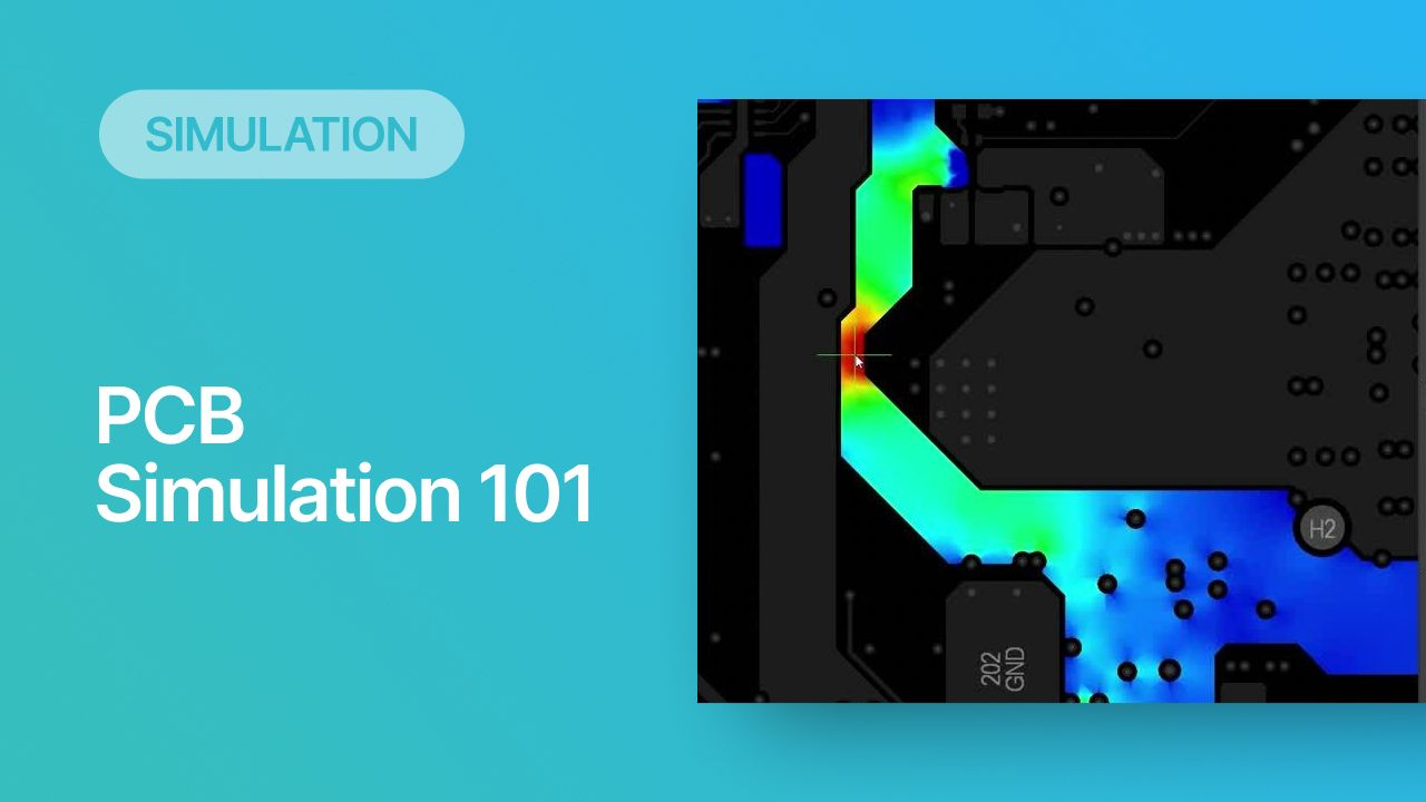
One simple but important simulation that should be performed in a finished PCB layout is DC power integrity analysis in your design's PDN. DC power integrity focuses on ensuring power is delivered throughout the design without resistive losses. Excessive resistive losses lead to high heat dissipation, so areas of the design where high current density and voltage drop are noticed can be targeted for changes. The typical solution is to add more copper, either by making the copper foil thicker or by increasing the width of polygons and traces.

The heat map shown in the above image displays the current density distribution in the power nets on the board. These nets carry different levels of current density, and regions of high current could indicate areas where high heat can be generated in the layout. These areas may need to be modified before the design can be sent for final evaluation and signoff. This type of simulation and others allow any of these remaining problems to be quickly identified and fixed in the PCB simulator layout.
AC power integrity is more complex, and it can be performed phenomenologically in SPICE simulations. Read this article for an example showing the basic structure of a SPICE simulation for examining power delivery in a PDN. AC simulation results depend heavily on the structure of a PDN in the PCB layout, which is a more advanced simulation requiring an electromagnetic field solver.
More Advanced PCB Simulations
The simulation tasks outlined above can all happen inside your electrical circuit design simulation software. These tasks all involve ensuring a design can be evaluated and qualified to the greatest extent possible before completion. The goal is to ensure any errors are caught before a design is submitted for signoff and especially before a design is placed into production.
Although it is ideal to fully simulate a design in a circuit tester program or other PCB simulator before production, some points in a design depend on the construction of the entire system, and they can't be simulated until a design is completed. Some of the most prominent examples include power integrity, EMI/EMC, mechanical reliability, and thermal management. These areas of design performance need to be simulated with a more advanced application called a field solver, which can solve the differential equations governing this physical phenomenon. In complex systems, multiple physical phenomena are interrelated and will need to be simulated together as multiphysics problems. Advanced PCB design software will include utilities that allow a design to be imported into these more advanced simulation applications so that system-level physical phenomena can be evaluated and quantified.
Some of the important simulations that can be run with a field solver application include:
- Parasitic extraction throughout a PCB layout
- Network parameter simulations that account for parasitics
- Near-field and far-field EMI simulations
- Heat generation and transport in a PCB layout, including into an enclosure
- CFD simulations to calculate and visualize airflow throughout a PCB and its enclosure
- Mechanical vibration and fatigue simulations targeted at specific components and interconnect.

The best field solver applications will operate with a realistic model of your PCB layout that you can export from your PCB design tools. To see some examples of Altium simulation tools you can perform and what you can learn from field solver simulations, take a look at the articles below.
- Learn more about impedance simulations inside a PCB layout
- Learn more about near-field EMI/EMC simulations
- Learn more about crosstalk simulations involving groups of nets
PCB component creation, sourcing, management, and much more are easy with the complete set of design features in Altium Develop. Altium also integrates with popular MCAD and simulation applications, giving you the ability to approach systems design while considering the mechanical constraints of your enclosure and components. It's the best electrical circuit design simulation software you can find. Experience Altium Develop today!

