


Designing Micro-vias with Sintered Paste for Rigid-Flex Printed Circuit Boards

At a Glance
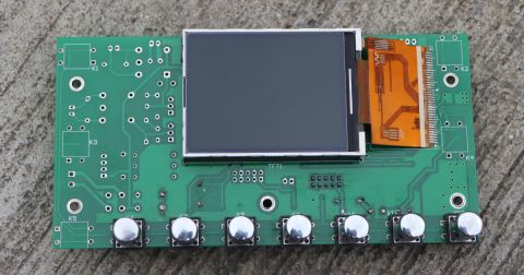
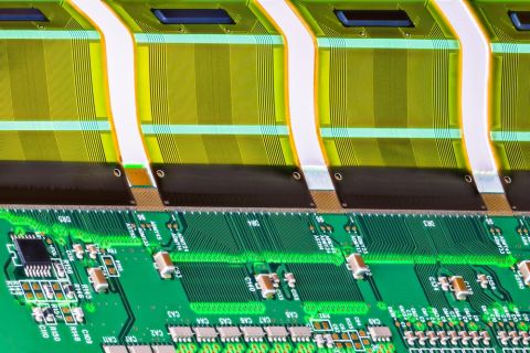
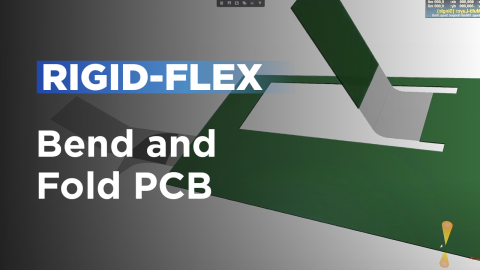
Rigid-flex Printed Circuit Boards (PCBs) are an elegant solution to many electronic packaging challenges. This technology brings together the durability of rigid PCBs with the versatility of flexible circuits. Rigid-flex PCBs are key to many modern devices such as smartphones, medical equipment, and automotive electronics


Rigid-flex Printed Circuit Boards (PCBs) are an elegant solution to many electronic packaging challenges. This technology brings together the durability of rigid PCBs with the versatility of flexible circuits. Rigid-flex PCBs are key to many modern devices such as smartphones, medical equipment, and automotive electronics. In these high-density routing applications, microvias are often used to interconnect different layers of the circuit board. A highly effective method for creating these connections involves using sintered paste. This blog explores the design rules and considerations for utilizing sintered paste microvias in rigid-flex PCBs.
First, let’s step back and define sintered paste in the context of printed circuit board fabrication. This refers to a conductive material composed of metal particles, typically silver or copper, suspended in a binder. The paste is applied to create electrical interconnections between layers of the PCB. During manufacturing, the sintering process involves heating it to a temperature below the melting point of other metal particles causing the particles to bond together forming a solid conductive pathway without melting the surrounding substrate.
Advantages of Sintered Paste Microvias
- Sintered paste microvias offer superior electrical conductivity compared to traditional plated vias. The sintering process reduces resistance, ensuring efficient signal transmission. This is critical for applications requiring high-speed data transfer and reliable performance.
- The capability to create smaller and closely spaced microvias allows for higher circuit density. This miniaturization is essential for developing compact and lightweight electronic devices without sacrificing functionality.
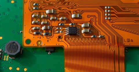
A common application of sintered paste microvias is routing into/out of a fine-pitch BGA on a flex substrate. These microvias can be very small in diameter (see below), which makes them an excellent option for this type of design. The sintering process also produces vias with high mechanical strength, making them resilient to the stresses encountered in both rigid and flexible sections of rigid-flex PCBs.
Key Design Considerations
Materials: Conductive Paste: Selecting the appropriate conductive paste is a key decision. Silver and copper-based pastes are commonly used due to their excellent electrical properties. Compatibility with the sintering process and the substrate material is essential.
Substrate Material: Rigid-flex PCBs use a combination of materials, such as FR4 for rigid sections and polyimide for flexible areas. Both materials must withstand the sintering temperatures without deforming or degrading.
Package Size: In HDI design on flex PCBs, the size of any fine-pitch packages will limit the available via size and routing space. Sintered vias overcome this challenge by enabling the smaller microvias mentioned above. An example is the Nordic WLCSP package (0.35 mm pitch) shown below; replacing the conventionally placed blind/buried microvias with sintered vias could allow routing between the pins.

Material selection is a time to work with your preferred printed circuit board fabricator. Not all fabricators work with all the available materials and processes. It is very simple to add additional cost and lead time to a project without understanding what materials are in stock and routinely processed.
Microvia Dimensions
Via Diameter and Aspect Ratio: Laser-drilled microvias typically range from 25 to 75 micrometers in diameter. Maintaining an aspect ratio (depth to diameter) around 0.75 to 1 ensures reliable filling and sintering of the paste.
Pitch and Spacing: To avoid electrical shorts and maintain signal integrity, the minimum spacing between microvias should be at least twice the via diameter. Adequate spacing also facilitates better heat dissipation.
Printed circuit board fabricators typically have these parameters listed in their manufacturing capabilities and design for manufacturability guidelines.
Design for Manufacturability (DFM)
Layer Stack-up: When designing multi-layer rigid-flex PCBs, consider the stack-up configuration to optimize the placement of microvias. Staggered vias can reduce stress concentration and improve mechanical robustness.
Alignment and Registration: Precise alignment during manufacturing is critical to ensure that stacked microvias connect accurately between layers. Advanced imaging and drilling technologies can help achieve this precision. Capabilities vary widely amongst fabricators, be sure to understand your preferred fabricators capabilities. Designing with those in mind saves cost and lead-time.
Thermal Management: Efficient heat dissipation is important, especially in high-density designs. Utilizing thermal vias and proper layout techniques can help manage the thermal load and prevent overheating.
Sintering Process Parameters
Temperature Profiles: Sintering temperatures typically range from 200°C to 300°C, depending on the paste and substrate materials. Controlled ramp-up and cool-down rates prevent thermal shock and material damage.
Time and Pressure: Sintering times vary from a few minutes to several hours. Applying pressure during sintering can improve paste compaction, reducing voids and enhancing the mechanical and electrical properties of the vias.
Atmosphere Control: Conducting the sintering process in an inert or reducing atmosphere, such as nitrogen or forming gas, prevents oxidation of the conductive paste, ensuring better electrical performance.
It is important to understand the key process variables that your fabricator needs to control.
Testing and Validation
Electrical Testing: Post-sintering, the electrical conductivity of the microvias should be measured using techniques such as four-point probe testing to ensure they meet design specifications.
Mechanical Stress Testing: The mechanical robustness of the microvias can be evaluated through bend and flex tests, ensuring they withstand the mechanical stresses encountered in real-world applications.
Reliability Testing: Long-term reliability under various environmental conditions, including thermal cycling, humidity, and vibration, should be assessed to guarantee the durability of the rigid-flex PCBs.
Common Challenges During Fabrication
Adhesion Issues: Improving adhesion between the sintered paste and the substrate is key for reliable vias. Surface treatment techniques, such as plasma cleaning or applying adhesion promoters, can enhance the bond strength.
Void Formation: Voids in the sintered paste can compromise the electrical and mechanical properties of the vias. Optimizing the paste formulation and sintering parameters, along with applying pressure during sintering, can minimize void formation.
Cracking and Delamination: Mechanical failures such as cracking and delamination can be mitigated by careful material selection and optimizing the design to distribute stresses evenly. Using flexible adhesives and substrates with matched thermal expansion coefficients can also help.
At the end of the day, sintered pastes are not new in PCB design, especially in HDI builds. This approach has been used to reach very high layer counts with fine feature clearances alongside fabrication of sintered paste vias. To learn more, watch the podcast episode below with expert Chris Hunrath:
Sintered paste microvias provide another tool in the PCB designers toolbox. Working with and understanding the capabilities of your PCB fabricator is a key component for success with this technology. Preferences for materials and processes vary greatly between fabricators and working together early in the design process can both save time and cost and improve reliability of the final product.
About Author
Related Resources
Related Technical Documentation
Table of Contents
Design to Release, Without the Friction
- Keep reviews tied to the right version
- Reduce handoff confusion and rework
- Spot sourcing and release risk earlier
- Work solo, share when needed
Get Started
Thank you, you are now subscribed to updates.

