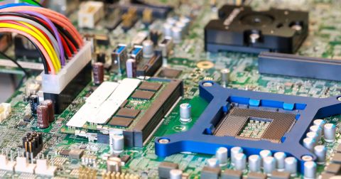


DIY Differential Oscilloscope Probe Project

At a Glance
Do you need a differential probe for your oscilloscope? Join Mark Harris designing a DIY differential probe, and exploring the advantages of using a differential probe for testing your circuit.


Let’s build a DIY differential oscilloscope probe! Sure, I could buy one, but where is the fun in that? I’m working on a big project that will require an LC Tank circuit to be tuned, this tank circuit simulates to have voltages exceeding 1000v peak to peak. Furthermore, the point I need to measure the voltage is across a capacitor, with neither side being earth ground referenced. This rules out simply using a high-voltage oscilloscope probe to measure the voltage. To measure this with standard single-ended probes, I would need to measure both sides of the capacitor with reference to ground, then use the math function in my oscilloscope to find the difference between the signals. While that is possible, it does lose resolution and more importantly for my application, use two of my four channels.
In this open source project, I’m going to attempt to build a 250MHz differential oscilloscope probe with a 1200v peak input voltage. The 250MHz bandwidth is very much a “hope for” spec, rather than a hard requirement, my immediate application for this diff probe only requires 100kHz of bandwidth. I don’t have the test equipment to generate a 250MHz waveform, therefore that specification is purely based on simulations. As with all my projects, you can find the design files on GitHub released under the permissive open-source MIT license.
Did you know that Altium has an all new spice simulation engine? If you have not tried it yet, sign up for a free trial of Altium Designer, or talk to an Altium representative about how integrating simulation directly into your simulation can save you from making mistakes!
This active probe uses high performance operational amplifiers, which require a dual supply voltage to be able to work with the input signal ranges. In my last project article, we built a separate power supply that runs off a 9v battery specifically for powering an op amp like this.
What is a Differential Oscilloscope Probe?
First, let's discuss what a “normal” oscilloscope probe is. The oscilloscope probes you likely use most commonly is a single ended probe, with a ground lead or spring which you connect to the ground of your circuit, and a pokey bit (technical term!) that you measure your signal with. If you were to connect that ground lead to something other than either a floating voltage or the same potential as your oscilloscope’s earth ground, you are very likely to damage the diff probe or oscilloscope. I hate to admit it, but I have done this in the past when probing a H-Bridge circuit, I completely vaporized the scope ground lead and melted the entire probe cable as it shorted my very high current h-bridge to ground through the scope. Not a great day at the office.
If you wanted to measure something such as a high side current sense resistor, you must use two single ended probes and a math channel to measure the voltage drop. If you simply connected the ground lead of your probe to one side of the resistor, and the tip of your probe to the other, you too would have a bad day at the office. While the load side of the resistor has seen a voltage drop, its potential relative to ground is still effectively the supply voltage - which would short your supply voltage through the current sense resistor to ground. If this supply voltage is very low resistance well, your oscilloscope lead is going to be rapidly converted to gaseous copper/PVC and you may well cause some catastrophic damage to your oscilloscope.
The correct way to measure the difference between two non-ground potential voltages is to use a differential probe. A differential probe is an active device which uses a differential amplifier to measure the difference between two signals. Neither of the inputs are referenced to ground, so the diff probe will only compare them to each other, then output a signal that your oscilloscope can use.
There are other uses for a differential probe too, it can allow you to see a waveform sitting on top of another differential signal, such as powerline ethernet.
Design
The design concept for a DIY differential probe is fairly simple. First, the input signal must be brought within the range of the amplifier inputs, then compare the two input signals to output the difference between them. Luckily, we don’t need to worry about power supply on this board, as it’s already taken care of in the form of my last project, which just plugs straight into this board providing all the power I require.
Schematic
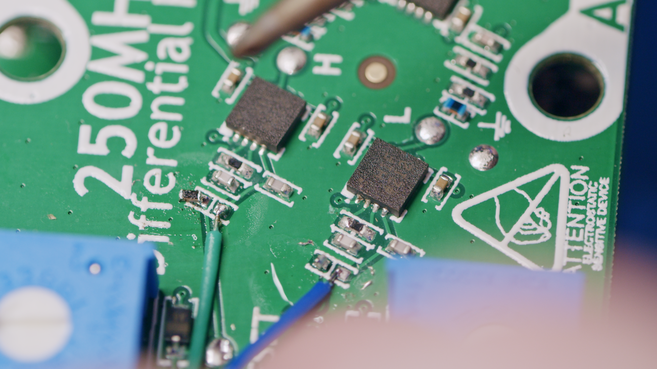
For the 1200v input probe, we start out with a voltage divider. This will make the probe a 500:1 probe, with a 5 million ohm input impedance. Each of the resistors and capacitors making up the 5 million ohm input is a 1206 surface mount resistor rated for 300V, which also provides our voltage isolation. If we used a single 5 million ohm resistor, there’s a strong chance that the distance between terminals would allow the input voltage to arc across the air gap, by passing the resistor entirely. By building a long chain of series resistors, the input signal would have to jump 5 gaps, which is unlikely to occur as long as the signal is remotely close to the maximum designed input voltage.
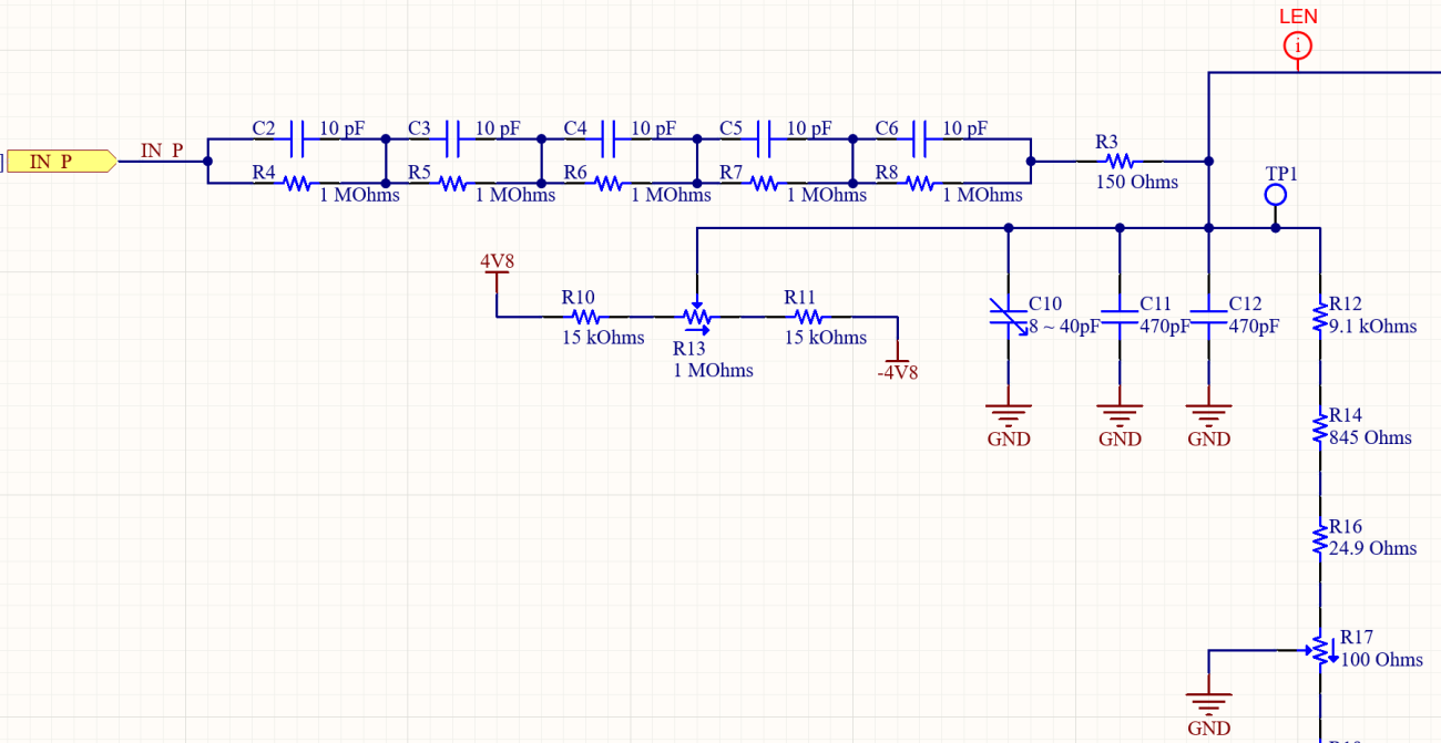
Multiple resistors are used for the low side of the potential divider to allow for the most precise measurement and tightest tolerance. Each of the resistors in the design is also 0.1% tolerance. The voltage divider should give us a peak output of +/-2.4V, which is safely within the span of the operational amplifiers.
On the divider we also have a trimmer pot (R13 above) for introducing a DC bias to the signal, allowing for input offset matching. The two input voltage dividers meet at a 100 ohm trimmer pot (R17) which allows the signals to be matched to each other.
Both of the inputs have matched signal paths. Every component and connection on one input is mirrored on the other. Choosing components with very tight tolerances is important, as any voltage differential between the two channels will be output as a signal. If we were measuring two signals carrying a common noise, such as EMI collected on a cable, we want to ensure that the levels of the two inputs are as near to identical as possible to ensure those matching signals do not show up on our output.
The output from the voltage divider is fed into an operational amplifier acting as a buffer amp.
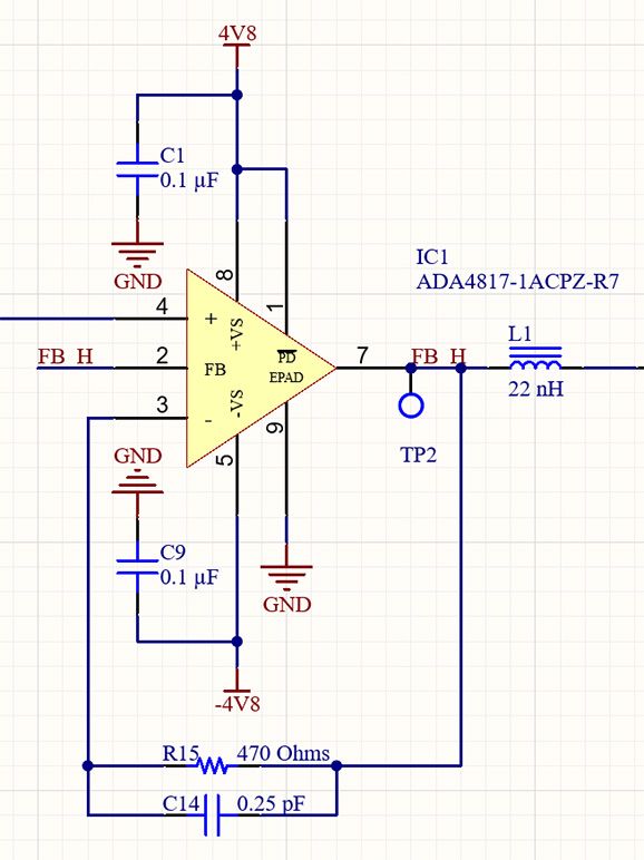
The Analog Devices ADA4817 were the highest-performance operational amplifiers in stock at the time of design. As a note on the capacitor in the feedback loop, the capacitor value in simulation makes a substantial difference for the response of the actual waveform, however, when testing in the real world, values from 0.25pF to over 18pF didn’t really impact the signal’s response as much as I’d hoped. The difference was almost negligible when switching from a 0.25pF capacitor to an 18pF - however, this could definitely have been my test setup. Similarly, the 22nH inductor was added to dampen ringing on the buffer amplifier outputs at high slew rates, however in the real world that slight ringing did not exist in a way that I could measure.
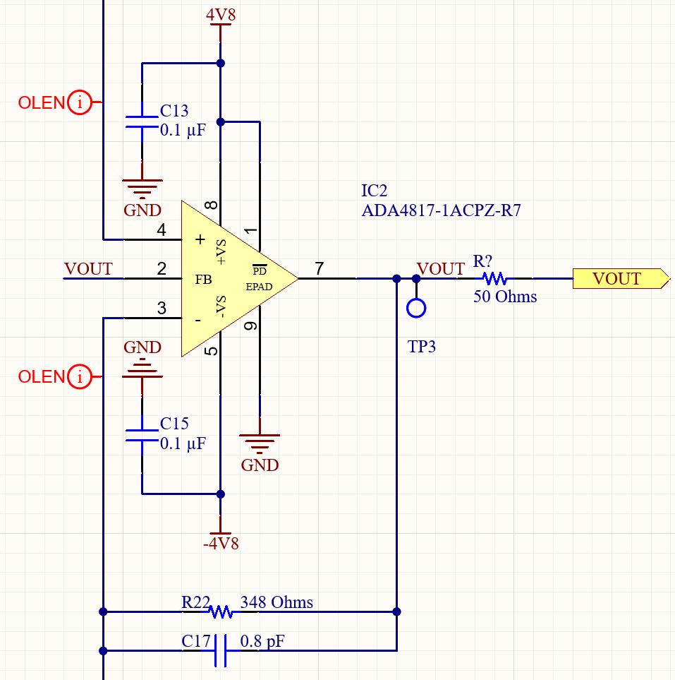
The two buffer amplifiers then feed into the differential amplifier (also an ADA4817) which outputs the difference between the two signals. The output from this third amplifier is ground referenced and sent to the oscilloscope. The output from the differential amplifier will go to a BNC connector, so standard coaxial cable with BNC connectors on either end can be used to connect the probe to an oscilloscope channel. The onboard battery makes it so only one cable is required, saving my workbench from further cable tangles.
The inputs to the board are SMA connectors. There are few, if any SMA connectors rated for 1200V input, therefore two connectors are used. The conductor of each connector is used as the signal input, with the coaxial shield able to be either floating (e.g.: for connection to ground on the Device Under Test), directly connected to board ground, or connected to board ground through a resistor. Pads for a 1206 size SMD resistor are provided to allow the selection of termination.
Alternatively, the SMA pad could be used with a probe socket to mount a range of spring probes. My concept for the SMA connectors is to create boards which can be connected to the diff probe with appropriate spacings for pogo probes to make contact with various sizes of SMD components. The SMA connectors will provide a secure connection that can be easily swapped.
Board
In order to get every bit of performance possible out of this design, I’m implementing high speed design practices that are quite excessive for the maximum frequency of this diff probe.
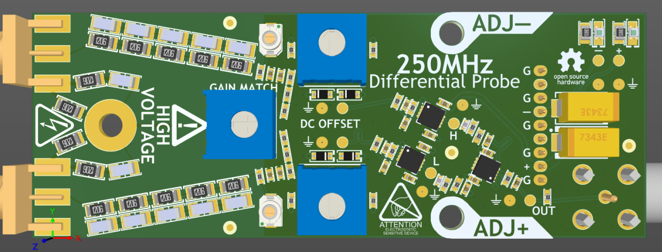
Firstly, as much of the signal chain as possible if placed on an angle. This strategy helps to ensure both signals travel across an equal amount of fiber and resin in the FR4 substrate. Why is this critical? The fiber bundles and epoxy have different dielectric constants/relative permittivity, so much so that you can see the difference when using a time-domain reflectometer to look at a signal passing through a microstrip over a fiber reinforced board. This is why boards with critical signals will specify spread glass, or flattened glass when using FR4 boards - or simply jump to a substrate with no reinforcements such as PTFE if the budget allows. By placing the signals on an angle across the fiber, the signals will still experience losses with budget boards, but the chances are the signals will have equal losses and delays.
To continue this concept, I’m also length matching the inputs to the amplifiers. By placing the amplifiers on an angle, the signal from each input has a non-equal distance to travel. The difference is only a dozen picoseconds or so, which I don’t think the amplifiers would even notice, but I’ll take any excuse to overdo things!
The board is also 4 layers, with two inner ground planes to ensure signals on the outer layers have a high quality return path. I’ve also ignored the whole idea of 90/45 degree traces, and had a lot of fun just directly connecting signals with “any angle” tracks by the shortest route.
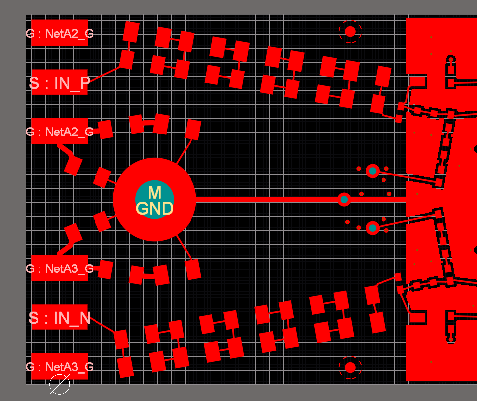
One thing you might notice is that I’ve removed the board’s scope ground plane from under the input voltage dividers. This was definitely a choice that I debated over a lot, ideally there should be a return path under the signals, but at the same time I want to reduce capacitance to board ground on that high voltage signal. The ideal solution would be to provide a return path back to the device under test under the voltage divider, but that won't always be possible. In the end, I decided to go without ground for that section of the board. Removing a return path from under a high speed signal should only be done after a lot of deep soul searching and is not recommended for the vast majority of applications.
The clearances on this board at the input are insufficient to meet IPC recommendations at the maximum voltage for an uncoated PCB. If using the board for 1200 volts input, the input stage should be conformal coated in order to ensure there is sufficient creepage/clearance distance.
Prototype Testing
I thought the design of this board was going to be the “hard” part of this project, and that prototype testing would be absolutely trivial. Of course, I completely misjudged this aspect of the project by ignoring the limitations of my test equipment when coming up with design requirements for the probe. It’s all well and good to design something to meet a certain performance characteristic, however it's somewhat futile if you have no way to qualify that performance.
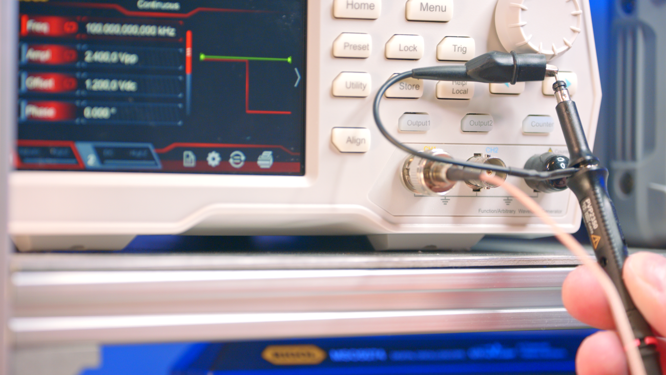
While I need the design to work to 1200V, I don’t actually have a way to test it to 1200V. My function generator can only generate a 10 volt peak to peak signal, and my lab power supply can only give me 64 volts peak. With my function generator only providing a maximum signal of less than 1% of the total design range, the output signal was incredibly weak and easily swamped by any EMI or other noise source. On top of that, both my standalone function generator and the one integrated into my oscilloscope are limited to generating a 25MHz squarewave. While my standalone generator can provide a 100MHz sine wave, this only has a 2 volt peak to peak signal which is even more challenging to measure on the output.
I’d like to say I quickly came to the realization that I needed to change my test approach… but I didn’t. I had tunnel vision of testing the probe from front to back and kept trying stupid ideas for generating a signal I could test with.
In the end, I finally realized I needed to qualify the voltage divider and operational amplifier sections separately. By separating testing of the two sections, I can feed a 2.4 volt peak to peak signal into the amplifier in order to test it. This is a much more manageable voltage for my test equipment, allowing me to progress with testing much quicker.
To facilitate getting a signal into the circuit, I removed the resistor that forms part of the RC low pass filter prior to each buffer amplifier. This allowed me to solder a 32ga wire to the pads, and then connect that to an SMA connector to make it easy to connect to my test equipment without having long, unshielded wires. Maximizing signal to noise ratio at this point is critical to seeing what the circuit is actually doing.
One issue I faced when testing was that my function generator carries a fairly substantial amount of conducted and radiated noise on its ground connections.
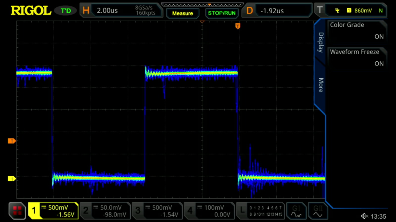
This sits around 120kHz, and is unnoticeable when probing its output with a single ended connection. However, with a differential amplifier it is a completely different story. The differential amplifier does not care that we consider the shield of a BNC/coax cable “ground”, because it is simply comparing the two signals coming into it. This leads to a large amount of spurious noise on the output signal of the probe. I spent a lot of time trying to determine where in my circuit this noise was coming from, only to accidentally notice my scope was showing some of this noise when the probe was sitting on the coaxial cable.
Switching to the function generator in my oscilloscope immediately rectified the issue, but limited me to a 25MHz maximum frequency. Interestingly, this did prove the differential aspect of the probe quite well, as the noise on the function generator’s ground was very visible in the differential output.
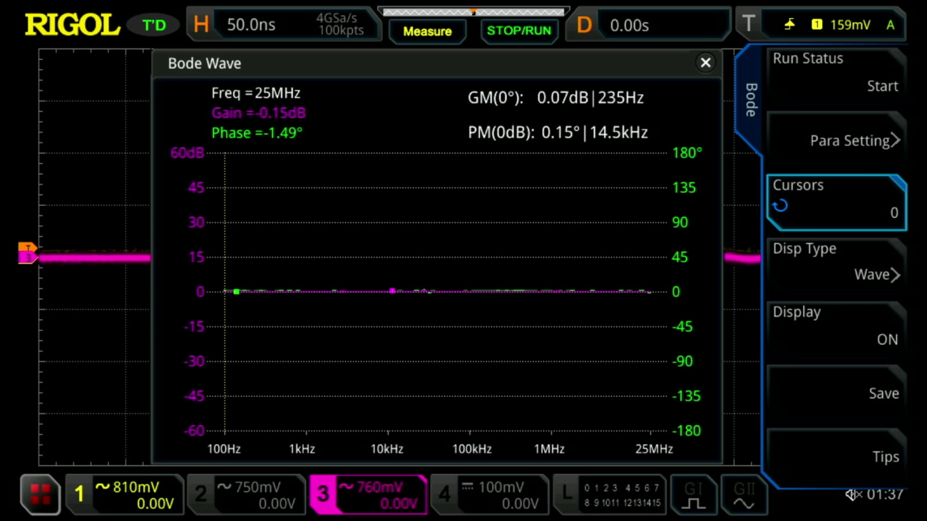
Using the Bode plot function of my oscilloscope, I was able to check the response of the first 25MHz of the probe’s response. It’s effectively a flat line, which makes me very happy. As mentioned above, I only need this to work to 100kHz or so, rather than the full 250MHz design goal.
Taking the Design Further
This design is not perfect. Building a 50:1 version by changing the low side resistors on the input divider allowed me to do some testing from end to end, and while the response is pretty flat across the frequency range I can easily test, providing a very fast edge of less than one nanosecond did show some issues with settling on the output, though the frequency of that edge is far beyond the designed range.
EMI shielding would be a fantastic addition to the design, significant issues with EMI were seen during testing - an RF Can covering amplifiers would be very welcome. Additional filtering for EMI would also be advantageous, assuming it does not impact the frequency response.
As mentioned earlier, the Altium Designer project files are available for this project, feel free to download them and see how you would beat my design. Don’t have an Altium Designer license? Sign up for a free trial today to see what all the fuss is about!
Testing this board gave me a lot of insight into how I can improve the design, which I’ll be embedding directly into an upcoming project with some changes of my own. This implementation will be subjected to enormous magnetic and electromagnetic interference, so will have a machined aluminum block for an RF shield rather than a mere sheet metal can.
About Author
Related Resources
Related Technical Documentation
Design to Release, Without the Friction
- Keep reviews tied to the right version
- Reduce handoff confusion and rework
- Spot sourcing and release risk earlier
- Work solo, share when needed
Get Started
Thank you, you are now subscribed to updates.

