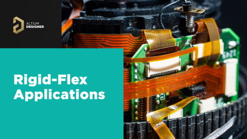
Flexible Circuit Assembly: Thinking Through Component Placement

As you would imagine, flexible circuits are ideal for applications that require a PCB to be thin, small, and light weight. Because of the thin, lightweight nature of the materials, they also present challenges for fabrication and assembly. Today’s blog is going to give a high-level look at some of these challenges and zero in on component selection and placement and how that can make or break the flexible circuit in application.
Placement in Flex PCBs
PCB designers should carefully consider component placement when designing flexible circuits, as the flexibility of the substrate introduces unique challenges during both fabrication and assembly. Wrong placement and orientation of components with respect to bending regions creates a reliability challenge, both in the case of static and dynamic flex.
Here are key considerations and risks to keep in mind:
Component Type and Size
-
Choose components that are suitable for flexible circuits, considering their size, weight, and mechanical robustness. Large or heavy components like large processors or power electronics components (inductors, transformers, etc.) will introduce additional stress during flexing.(We will be getting into this in more detail below)
Solder Joint Location
-
Flex regions should not be located near solder joints in order to avoid excess stress and cracking during bending. Inflexible solder joints may fracture when the circuit bends, leading to electrical failures.
Flexible Trace Routing
-
Route traces in bend regions with gentle curves and keep sharp bends away from the bend regions. Sharp bends could shear more easily than curved traces during flexing.
Stiffeners and Supports
-
Integrate stiffeners strategically to provide additional support in areas prone to mechanical stress. Examples include regions with large components, mezzanine connectors, and board-to-board connectors.
SMT or Through-Hole
-
SMT components are most commonly used in flex PCBs, but sometimes through-hole components are used. Through-hole components may not have enough copper pad area to form strong bonds and so should be placed in regions with stiffeners.
Prototyping and Testing
-
Prototype flexible circuits to validate component placement, bending, thermal reliability, and mechanical reliability. Make sure to qualify the flex design in an MCAD application, or even in a dynamic stress simulation. Failing to analyze dynamic stress may result in unexpected failures during or after assembly.
Addressing these considerations, PCB designers can mitigate risks associated with flexible circuit manufacturing and ensure that the designed components can withstand the unique challenges posed by the flexibility of the circuit materials.
Size
-
Miniaturization: Opt for smaller-sized components, when possible, as they distribute less mass and reduce the risk of introducing stress points during flexing.
-
Package Size: Choose components with compact package sizes to minimize the impact on the overall flexibility of the circuit.
Weight
-
Lightweight Materials: Prioritize lightweight materials for components, especially for applications where weight is a critical factor. Heavy components can increase the overall stress on the flexible circuit during bending.
-
Low-Profile Components: Select components with low profiles to minimize the mass and height, reducing the potential for mechanical stress.
Mechanical Robustness
-
Flexible Designs: Design with mechanical robustness in mind ensuring the end product can endure the mechanical stresses associated with flexing without breaking or deforming.
-
Reinforcement: Consider reinforcing areas around components that are prone to mechanical stress, either through additional substrate layers or strategically placed stiffeners.
Large or heavy components may introduce additional stress during flexing, leading to reliability issues.
Stress Concentration
-
Mechanical Stress: Large or heavy components can create stress concentration points during flexing, potentially leading to cracks in solder joints, traces, or the flexible substrate. The increased mechanical stress may result in long-term reliability issues, including fatigue failure or delamination of the flexible circuit.
Impact on Flexibility
-
Reduced Flexibility: Heavy components can limit the overall flexibility of the circuit, making it more challenging for the circuit to conform to the desired shape or bend radius. Restricted flexibility can impact the performance of the flexible circuit, especially in applications where repeated flexing is a requirement.
Assembly Challenges
-
Handling Difficulties: Large or heavy components may pose challenges during the assembly process, requiring careful handling and specialized equipment. The weight of components can affect the quality of solder joints, potentially leading to issues such as solder joint cracking or misalignment.
Material Compatibility
-
Material Strain: Heavy components may cause strain on the flexible substrate material, affecting its mechanical properties over time. Continuous strain may contribute to material fatigue, reducing the overall lifespan and reliability of the flexible circuit.
Design Iterations
-
Prototyping: To mitigate long term risks, conduct prototyping with a focus on assessing the performance of large or heavy components during flexing.
By carefully considering the type, size, and mechanical characteristics of components, PCB designers can optimize flexible circuit designs to ensure reliability and performance, particularly in applications where flexibility is critical. As always, collaborating with manufacturers during the design phase can help identify and address potential issues associated with component placement on flexible circuits.
About Author
Related Resources


Related Technical Documentation


Take advantage of the world's
most trusted PCB design system.
One interface. One data
model. Endless possibilities.
Effortlessly collaborate with
mechanical designers.
The world's most trusted
PCB design platform
Best in class interactive
routing
View License Options
Thank you, you are now subscribed to updates.