


Easily Create Your PCB Solder Mask Layer in Altium Designer


You’ve just finished the electrical layout of your board and now you are working through the final steps to prepare for PCB manufacturing and assembly. What steps do you need to take to get your board ready for production? Aside from generating deliverables like Gerber files, a bill of materials, drill files, silkscreen, and PCB assembly instructions, you’ll need to define the solder mask (sometimes called solder stop mask or solder resist) on the surface layers of your PCB. This important production planning step is much easier when you use the right PCB design software with a full suite of design tools in a single program.
ALTIUM DESIGNER®
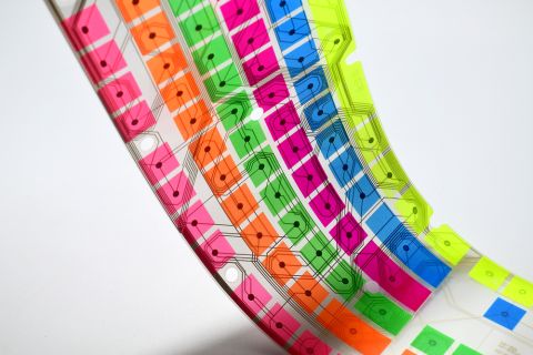
The only unified PCB design package with a complete set of PCB design and layout tools for rigid, flex, and rigid-flex boards.
Understanding the appropriate board design process for how to solder mask a PCB is a critical step before PCB manufacturing and assembly. This coating is applied to the surface of a PCB and ranges in variety from epoxy solder resist to UV photoimageable solder mask. It also gives your circuit board the color and look you want once it comes off the assembly line.
Placing the right solder stop mask takes the right set of CAD tools for printed circuit board design. The CAD tools in Altium Designer are built on a single rules-driven design engine with a unified data model. This lets you easily define your solder mask clearance and pad opening. You’ll also have a complete set of design tools for PCB manufacturing and assembly, both for rigid and flexible printed circuit board designs.
What is Solder Mask and Why Does My PCB Need It?
PCB solder mask (also called solder resist) is an epoxy or photoimageable polymer layer that protects copper on the surface layer of the PCB. This layer covers exposed traces on the surface of the board, preventing oxidation and providing an extra protective barrier against mechanical damage.
Solder resist provides another benefit to your board; it helps prevent unintended connections from forming during assembly when components are soldered onto pads and holes. A solder bridge forms when two pads on a board or two leads on an IC package are unintentionally soldered together, which typically happens due to the use of too much solder paste during assembly. Defining the right solder stop mask opening size and thickness helps ensure that solder remains on a conductive pad during wave soldering. This also helps prevent tombstoning of components on the surface layer.
How the Solder Mask Process Affects Your PCB
Solder mask was created primarily to facilitate wave soldering during mass assembly. Proper use of solder resist is critical for ensuring proper wave soldering and unintended solder bridges during assembly of rigid circuit boards. As modern boards require higher trace density routing and component placement, PCB solder mask is something of a requirement rather than an option in most boards.
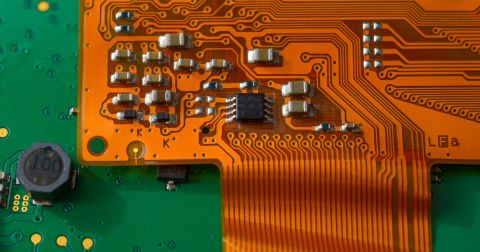
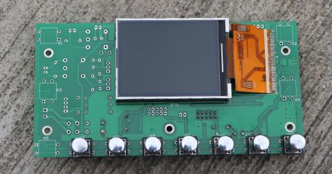
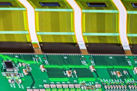
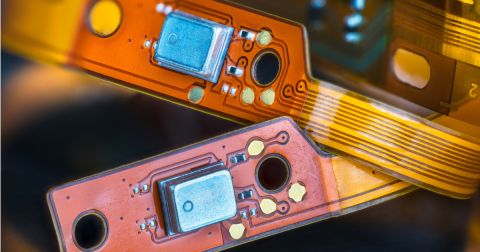
With flex ribbons in rigid-flex PCBs, or with fully flexible PCBs, you’ll need to decide whether to use flexible polyimide coverlay or flexible solder mask to protect critical traces on a polyimide substrate. The answer to this important question really depends on whether you intend to solder components directly to the flex ribbon and the level of flexibility required on the finished PCB.
- Should you use an epoxy-based, lacquer-based, or photoimageable polymer-based solder mask in your board? The answer depends on industry standards, required solder mask thickness, and the level of surface complexity.
Learn about choosing the right solder stop mask for your next PCB.
- In addition to solder mask, there are other options for preventing corrosion on exposed conductors in your PCB.
Learn more about methods for preventing corrosion in exposed PCB traces.
- With flex and rigid-flex circuits, you’ll need to decide whether to use a flexible solder mask or polyimide coverlay to protect traces on a flex ribbon.

3D view of a PCB with blue solder mask layer and silkscreen in Altium Designer
What Should Appear on the Solder Mask Layer and Stencil
Your solder mask layer will be defined in a Gerber file along with your other electrical and mechanical layers. Silkscreen printing is another important aspect of preparing for assembly and will be placed after the solder mask has been placed and cured. Clearance and printing requirements on silkscreen on the surface layer of a circuit board are specified in the IPC standards.
The IPC-SM-840D standards define solder resist requirements for a printed circuit board intended for use in certain industries or applications. A lot number and a unique manufacturer’s mark will need to be placed on the board using silkscreen in order to provide traceability in the event of a recall. Make sure to allocate space on your circuit board for this information and clearly specify this in your design.
Generating Gerbers and PCB Manufacturing Files With Solder Mask Stencil
Printed circuit board software tools create a stencil layer within the Gerbers. This is used during fabrication when applying the solder stop mask material. Stencils are specified for dimensioning the solder mask interface to its intended openings and clearances. Dimensional requirements include specifying expansion metrics to create the shape at each pad and via site that should be excluded from coating. Once the shape is defined, clearances are set up to define minimum clearance spacing in your circuit board.

Define a PCB solder mask rule for expansion or contraction at the conductor

Use clearance rules to ensure silk screen expands just beyond the edge of conductors
You can prevent unintended bridging during assembly when you apply the right clearances in your printed circuit board design rules. Solder mask coating is applied during the final stages of fabrication with a stencil placed, and the stencil will match the parameters you define in your PCB layout. When your design software includes PCB manufacturing documentation tools alongside your design rules and CAD features, you can rest assured you’ll avoid common solder resist problems.
- Placing the right solder mask clearance is an important aspect of DFM for wave soldering.
Learn more about PCB fabrication and assembly with wave soldering.
- Your solder stop mask is important for preventing other SMD process errors. Be sure to check your Gerber files for common SMD mistakes before PCB manufacturing.
- The major SMD process error solder mask helps prevent is accidental shorts during wave soldering or hand assembly.
Learn more about solder bridge shorts and how your design rules help prevent them.
Altium Designer Specifies Mask and Manufacturing Rules for Soldering
Altium Designer provides a complete set of tools for specifying solder mask clearances and your silkscreen layer. You can use the PCB Rules and Constraints Editor to define important PCB manufacturing rules for your solder mask. The rules allow a definition of mask expansion or contraction with respect to each pad and via site. Once expansions are defined, you scope manufacturing rules to include minimum width restrictions for successful application of solder in narrow regions between pins and other objects.

Set up minimum dimensions for solder resist clearance requirements.
The design features in your PCB design application should let you do more than just set clearances for solder resist around pads and vias. Your CAD tools need to interface with a complete set of design features for routing and high-speed layout, as well as automated rules checking features for your layout and schematic. This is the type of environment you’ll find in Altium Designer, the only application that unifies design, layout, and PCB manufacturing features into a single platform.
Design Rules Help You Manage Clearances and Solder Mask
The rules-driven design engine in Altium Designer is ideal for creating schematics and your layout, as well as preparing circuit boards for manufacturing and assembly. Everything you need to prepare a real board, including solder mask and silkscreen layers, is included in Altium Designer. Best of all, you won’t have to switch between different applications to create your manufacturing documents, everything you need is in one place.
- The CAD tools in Altium Designer’s rules-driven design engine allow you to accurately place components, verify PCB solder mask clearances, and examine your solder mask without using a separate program.
Learn more about the unified PCB design features in Altium Designer.
- Silkscreen is one important aspect of design that will need to be placed on top of your solder stop mask. You can easily verify silkscreen to solder mask clearances and other clearances in Altium Designer’s PCB editor.
See how you can define silkscreen to solder mask clearance in Altium Designer.
- Once you’re ready to prepare for manufacturing, you can define solder resist expansion and other important aspects of your board to prepare for PCB manufacturing.
Learn more about creating your solder mask in Altium Designer.

Preparing Gerber files and assembly drawings in Altium Designer
Solder stop mask is one of those all-important design steps that designers must complete prior to sending circuit boards off for PCB manufacturing. Altium Designer gives you intuitive command structures for designing PCB solder mask sets. With easily accessible editors, you can set solder resist expansions, or contractions, along with manufacturing clearances that define the stencil. With the stencil designed and available in the Gerber files, you’re confident that the board will be protected from contamination and free of solder bridges.
Altium Designer on Altium 365 delivers an unprecedented amount of integration to the electronics industry until now relegated to the world of software development, allowing designers to work from home and reach unprecedented levels of efficiency.
We have only scratched the surface of what is possible to do with Altium Designer on Altium 365. You can check the product page for a more in-depth feature description or one of the On-Demand Webinars.

About Author
Related Resources
Related Technical Documentation
Table of Contents
Design to Release, Without the Friction
- Keep reviews tied to the right version
- Reduce handoff confusion and rework
- Spot sourcing and release risk earlier
- Work solo, share when needed
Get Started
Thank you, you are now subscribed to updates.


