


The History and Use of Cross-Hatched Planes

At a Glance
Read to learn all about hatch ground in your PCB instead of using ground planes. You'll learn about how this type of ground region impacts signal integrity.


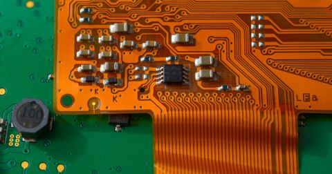
Cross-hatching of PCB planes refers to a method wherein certain planes or other large areas of copper within a PCB appear as a latticework of copper. Regular openings are placed at regular intervals, much like those that appear in a screen door. The requirement for cross-hatching a plane is rare these days in rigid PCBs, but they are used in flex and rigid-flex implementations where they can provide a number of benefits. So when is it appropriate to use hatching, particularly hatch ground or hatch power regions?
Although not so useful anymore in rigid PCBs, they've become quite important in flex/rigid-flex PCBs, where the hatch ground pattern plays dual roles as a structural support and a ground element. This article will describe the history of cross-hatch planes, how they are made, the reason they were initially used in rigid PCBs, and their ongoing role and benefit today in flex and rigid-flex boards.
Definition and History of Hatch Ground
As noted above, a hatch ground plane is a latticework of copper with regular openings at regular intervals. The actual process of creating a cross-hatched plane occurs in the CAD or CAM system, where the region to be hatched is the filled area with a series of regularly spaced lines much, like the traces plotted in signal layers. Then, the area is edged with a thin border trace that connects the ends of the lines that form the crosshatch. Connections, such as power or ground connections, are made to this cross-hatching in the same way that they are made in solid planes.
In the earlier days of the multilayer PCB fabrication process, the final step of inner layer processing involved roughening the copper surfaces so that they would adhere tightly to the resin in the prepreg system during lamination. This step was necessary because the copper surfaces as they emerged from the DES (develop, etch, and strip) process were very smooth. In fact, they were so smooth that it was difficult to create a strong bond between the resin used to laminate the PCB and the copper. As a result, if the copper surfaces weren’t roughened, delamination would occur between the laminate and the solid copper planes of the PCB. This same problem occurred with component mounting pads on outer layers resulting in pads coming loose from the PCB while soldering during rework.
Note: The same adhesion problem also exists when pieces of laminate are manufactured. The same resins, used in manufacturing a PCB, are employed during laminate manufacturing. Here, resin impregnated glass cloth is combined with a piece of copper foil bonded on each side to create the laminate. In this instance, the surface of the copper foil that is bonded to the resin gets its rough finish as part of the plating process that creates the foil.
Implementation in Rigid PCBs
To address the foregoing copper adhesion problems on rigid multilayer PCBs, cross-hatching was created. The actual process involved creating small openings in the copper plane so that the resin would bond to the laminate through the copper, rather than attempting to force a bond directly between the resin and copper. As long as the bond to the laminate was sufficiently strong and distributed throughout the board, the board would be study enough to resist delamination.
This basically solved the delamination problem but created an expensive proposition because of the complex CAD files that had to be created. Much like the beloved Gerbers of today, these files were used to describe layers and plot the film that was required to image those layers. During this time, CAD tools were nowhere near as powerful as they are today, and designers couldn't simply export these files with a few clicks of a button.
In the late 1980s, a new process was developed that solved the foregoing adhesion problem so that cross-hatched planes on rigid PCBs were no longer necessary. This process is accomplished through one of two approaches. One is called black oxide treatment, and the other is called alternative or brown oxide. After this step, the appearance of the copper on an inner layer is matte black following the black oxide approach or brown in color following the alternative oxide approach. An inner layer with black oxide is shown in Figure 1.

Both of these approaches micro etch the copper so that it is rough enough to bond with the resin in the prepreg. Essentially, they provide the “teeth” to which the resins can bond. The treatments are done to all inner layers after etching and just prior to lamination. The result is a very strong bond between prepreg resins and the layers of copper in a PCB.
Note: Copper roughness is often discussed as a problem with very high-speed signals due to increased skin effect loss in the traces of the PCB. In order to reduce the roughness of the copper trace surfaces an alternative surface preparation such as Atotech Bondfilm is used which does not increase the surface roughness.
Cross-hatching in rigid PCBs is rarely done these days. In fact, if a fabricator or other source asks for cross-hatching to be applied to inner layer planes or copper fills on outer layers, one of two things are at work:
- The fabricator or other source is operating with very old, outdated rules.
- The fabricator does not have adequate process control and should be avoided as a board manufacturer.
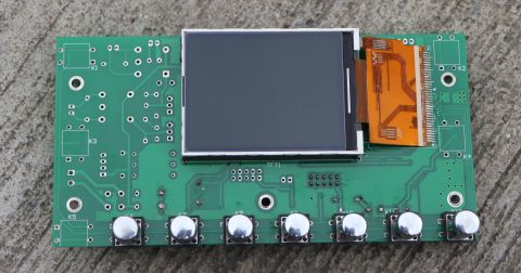
Cross-Hatching in Flex and Rigid Flex Circuits
While cross-hatching is rarely used in rigid PCBs these days, it does have practical application for both flex and rigid-flex circuits. These applications come in two areas for flex and rigid-flex circuits:
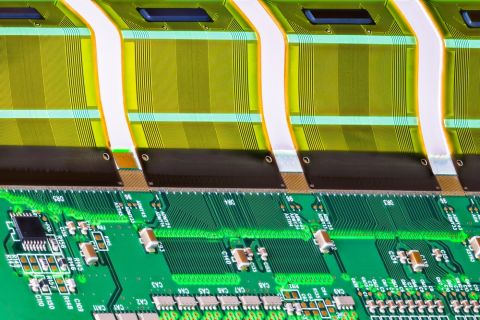
- Controlled impedance in flex regions: Using a hatch ground is a good method for providing the reference plane required in controlled impedance routing for high speed digital boards. The hatch ground provides wider, more manufacturable dimensions while retaining the flexibility of the circuit and assembly. It should be noted that cross-hatching reduces the amount of copper under a transmission line, which decreases the capacitance and raises its impedance.
- Structural support for flex regions: Using a hatch ground provides structural support needed for a dynamic or static flex ribbon without increasing the rigidity of the copper layer. on a two-sided flexible circuit. The layer can still be used for controlled impedance routing creating undesired rigidity, or the ribbon can be permanently deformed.
In order to calculate a trace width that results in the correct impedance, it is necessary to use a modeling tool that accounts for the missing copper in the crosshatched plane. Because the impedance for a given trace over a hatch ground region is higher than that over a solid ground region, the inductance of the trace needs to be decreased to maintain controlled impedance. Therefore, we would want to make the trace a bit wider as this will reduce the trace's inductance and increase the total capacitance with respect to the hatch ground. Both effects will contribute to set the impedance to the correct value.
Summary
There was a time when it was necessary to use hatch ground planes and pour as a way to guarantee proper adhesion of prepreg resins to the copper foils in rigid, multilayer PCBs. Poor adhesion to smooth copper resulted in delamination of the inner layers. However, this is no longer necessary due to the development of surface treatments that create a secure bond between the resin and copper. As a result, the use of cross-hatch planes in rigid multilayer PCBs have gone by the wayside. However, the use of this process in rigid-flex and flex circuits is of benefit as it ensures a polyimide region in a flex/rigid-flex board can remain flexible.
Would you like to find out more about how Altium can help you with your next PCB design? Talk to an expert at Altium.
References
- Ritchey, Lee W., and Zasio, John J., “Right The First Time, A Practical Handbook on High Speed PCB and System Design,” Volume 2.
About Author
Related Resources
Related Technical Documentation
Table of Contents
Design to Release, Without the Friction
- Keep reviews tied to the right version
- Reduce handoff confusion and rework
- Spot sourcing and release risk earlier
- Work solo, share when needed
Get Started
Thank you, you are now subscribed to updates.