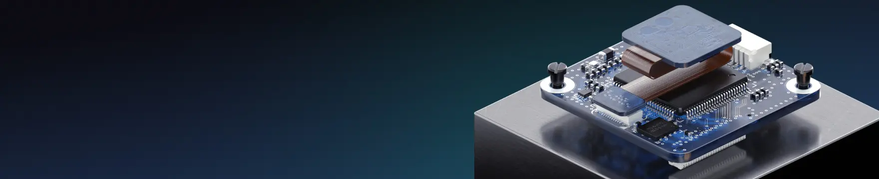
High Density PCB Design Game Changer: 25 Micron Trace and Space


Have you heard the latest development in PCB fabrication processes? High density PCB design follows the same trend seen in integrated circuits, where more functionality is packed into a smaller space. The smaller spacing in these boards makes precise manufacturing more difficult, which places important DFM rules on your high density PCB design.
Now with the A-SAP™ process, you can place trace widths and spacing down to 1 mil, allowing tight escape routing from very fine pitch BGAs. By focusing on reducing trace width and spacing, this process allows some interior layers in the stackup to be removed, which offsets the overall cost of this process.
A Couple Of High Density PCB Design Examples
Simplifying Complex HDI Routing
With tight BGA routing, the complexity of PCB designs can increase quickly. The A-SAP™ process resets that technology curve. Imagine a 12-layer design, requiring three sequential lamination cycles, using three mil line width and spacing. This design is complex and expensive. Each lamination cycle significantly increases costs and decreases yields. Now re-imagine this with the ability to route with a one mil line and space. Four of those 12 layers can be replaced with A-SAP™ layers, this change alone eliminates four of those original 12 layers, and perhaps even more exciting, the PCB is now able to be built with a single lamination process. This significantly reduces the complexity and cost of that design.
SWAP
The ability to route with one mil trace and space can also have a significant impact on space, weight, and packaging, something that many applications struggle with as we work to put increasingly sophisticated electronics in smaller and smaller packages. The overall length and width of the PCB could be reduced. The number of necessary layers could be reduced, which in turn reduces both overall thickness and weight. In many cases, both the overall size and the number of layers could be reduced. This is also interesting to look at from another perspective. Using one mil line and space, what additional electronic functionality could be added to an existing footprint?
How Does The Process Work?
Traditionally, circuit patterns on rigid PCBs, flexible circuits and rigid-flex constructions are created using a subtractive etch process. This process starts with copper-clad laminate, and through a series of process steps, any unnecessary copper is etched off that panel leaving the intended circuit pattern. Most often, this process is limited to three mil line and space.
The A-SAP™ process starts by completely etching away the copper from the base dielectric material. The dielectric is coated with LMI™, processed through electroless copper, processed through imaging and processed through electrolytic copper additively forming the intended circuit pattern. Because this is additive, the feature sizes can be much smaller than with subtractive etch, and there is improved RF performance because the trapezoidal effect of the etching process is eliminated.

Once the circuit pattern is created, the PCB layer is processed in the same way that a typical PCB layer is currently processed. The A-SAP™ process integrates with the imaging and chemical processes already being utilized for subtractive etch fabrication, which results in a low capital expenditure requirement to bring the process in-house. Cleanliness and handling become more critical, and PCB fabricators implementing this process comment that improvement in those two areas aids in overall yield improvement, including to layers being built with subtractive etch processing.
Let’s Get Creative
At this point in time, there are no standard design rules for the A-SAP™ process, and fabricators are advocating for a collaborative approach to design. Early designs have run the full gamut with everything from a simple single-layer design with two mil line and one mil space to a complex, stacked microvia, multiple lamination design, on mixed materials, adding in the complexity of one mil line and space to an already difficult build. Work is being done to help apply best practices for routing tight pitch components in the most optimal way. As with any new technology, there is a learning curve for the fabrication process and design for manufacturability. This is an opportunity to think more creatively, to identify possibilities and applications for 1 mil trace and space.
Here Are Some Thoughts And Ideas
While there are some benefits to reducing trace width and spacing down to 1 mil, there are some open DFM questions for high density PCB design. Although BGA escape routing is easier, there are new design questions that arise for HDI boards.
- With a one mil line and space, can you increase hole size, which allows you to increase material thickness or use mechanically drilled holes rather than laser-drilled holes?
- Does a 1 mil line and space allow you to maintain staggered microvias, rather than being forced into stacked microvia construction?
- Do you use all A-SAP™ layers?
- Do you use selective A-SAP™ layers? What are the advantages to this approach?
- Are there routing advantages at two mil line and space?
- Are there yield benefits to using the A-SAP™ process with three mil line and space on outer-layers (which is typically an area of yield and capability concern)?
- By how much can you physically shrink the size of the PCB routing with finer line and space?
- How many layers can you eliminate?
- How many sequential lamination cycles can be eliminated?
These thoughts and ideas are just barely scratching the surface of high density PCB design as we start to move through this learning curve. I am extremely curious for PCB designers to weigh in and comment with their thoughts on how this technology can be applied. I look forward to the comments on this blog post!
Have more questions? Call an expert at Altium or learn more about the best PCB router software for your complex designs.
About Author
Related Resources
Table of Contents
Design to Release, Without the Friction
- Keep reviews tied to the right version
- Reduce handoff confusion and rework
- Spot sourcing and release risk earlier
- Work solo, share when needed
Get Started
Thank you, you are now subscribed to updates.