


Getting Started With nRF52 MCU in a PCB

At a Glance
See how to get started with the nRF52 in a PCB layout. We’ll show how to use the fine-pitch BGA package version of this component.


Click here to jump to the viewer embed and browse this project
Most semiconductor manufacturers have developed and released their own line of microcontrollers, and Nordic Semiconductor is no different. One of their best-known products is the nRF52, an RF-capable SoC with an integrated transceiver. This component is small, offers a high I/O count, and has a part number that comes in a fine-pitch BGA package.
In this article, I’ll show a PCB layout example that uses the fine-pitch BGA package version of the nRF52. At the end of the article, you’ll have an opportunity to download the source files for this project. Without further delay, let’s get started with an example PCB layout that includes the nRF52.
For viewers who want to watch the entire design process for this component, we created the following playlist that guides users through the process of using the nRF52 in a PCB layout. Specifically, we cover how to use the high-density (0.35 mm ball pitch) version of this component in a design that requires some HDI design techniques. We’ll also show the entire engineering journey that got us to the final version of our nRF52 module.
Front-end Design
The nRF52 comes in a few different packages with small form factors. This chip has become popular as a Bluetooth-capable microcontroller with moderate pin count and standard digital interfaces, including the ability to use USB in the device. The component targets small embedded devices with Bluetooth 5 connectivity.
In this project, the component we will use is the nRF52840-CKAA-R7, a 93-pin WLCSP with a BGA footprint. This processor is known for running at low power when not broadcasting, so it is possible to use it with a small battery. We’ll add some battery regulation and polarity protection circuitry for this system so that it can successfully run with battery power.
nRF52840 WLCSP Footprint
The footprint for the nRF52840-CKAA-R7 is shown below. The measure bar between balls shows that the pitch is 0.35 mm pitch. This is a very fine pitch and it will require some design techniques used in HDI designs.

Other Important Components
We’ll get into the pinout and fanout for this component in one of the sections below. For now, there will be several other components that appear in the design:
- TPS70933DBVR - Low-current linear regulator
- FR015L3EZ - Low-side reverse polarity protector
- BD33HC0MEFJ-ME2 - 3V3/1A regulator for logic circuits
- PCF8523TK - Real-time clock (RTC) with I2C interface
- CAT24C512WI-GT3 - 512 KB EEPROM
The device will initially need to connect to a LiPo battery through a standard 2-pin connector, and we will need to include at least one header to access I/Os and program the board. The I/O count is larger than we would typically fit onto a single header, so it’s a judgment call as to whether to include a 2nd header only for accessing I/Os. For now, we’ll proceed with the battery connector and a single I/O header, and we can always add another connector later.
Getting Started: Schematics
The schematics for this device are not too complex and all the circuits will fit on a single page. I’ll show different regions of the schematics individually so that the entire design is clear and easy to read.
First, let’s look at the power section. In this device, 3V3 power is provided by a low-noise, low-current LDO with 150 mA rated current output. The LDO takes the battery power (VBAT) as an input and converts this to the desired 3V3 output.

Based on the net connections for VBAT and VDD1, we see that there are two ways to provide power to the board:
- Apply 3V3 directly to VDD1, such as through a pin header
- Apply voltage directly to the VBAT net, also through one of the connectors
In the former, you would only power on the MCU and RTC; there would be no power to the peripherals. In the latter, you would be providing power to the entire system, and now VDD1 would be an output rather than an input.
You’ll notice that a 2nd regulator is providing 3V3 power for net VDD2. This regulator includes an enable pin, so the device can power up first using VDD1, and then the peripherals (in this case, the EEPROM) can be powered up using VDD2. This gives the device the capability to turn off its peripherals when the device is not in use by toggling the VDD2_ENABLE pin. If we had any other peripherals we might want to include in this design that is not central to powering on the device, we would want to connect these to VDD2 instead of VDD1.
Next, let’s look at the nRF52840 connections. These were borrowed from the Nordic dev board and the original set of connections on their components can be accessed in their Altium design files.

Here I’ve broken out several interfaces, and the supporting circuitry mostly contains reference crystals and some capacitors. The caps range from a large case for bulk decoupling, down to a small case (0201) for bypassing on the VDD1 rail. There are still plenty of pins left over in this component, and these could be used for other peripherals. I’ll eventually break some of the additional I/Os and the SPI interface to a pin header as shown later in the video series.
If you take a look at pin E1, you’ll see the antenna connection. Initially, starting from the original schematics and layout in the reference design, this impedance-matching network used different output capacitor values. The impedance matching network shown below was determined by reverse engineering the antenna impedance with an online calculator and modifying the matching network so that it is symmetric. Swapping the 0.8 pF output cap in the reference design with the 1.2 pF output cap shown below produces essentially the same performance.

This essentially concludes the schematic capture portion, and the remaining circuits are simple to implement. We can now move into the PCB layout.
PCB Layout
Once in the PCB layout, we have a few important tasks to complete to use the nRF52840 in WLCSP:
- Determine a stack up and BGA fanout
- Place the antenna as a printed element
- Place and route the other ICs so they will not interfere with the RF section
Stackup and Fanout
The main driver of the stack-up and fanout strategy is the ball pitch on the nRF52 package. Readers may notice above that the ball pitch is 0.35 mm. The pad size in my footprint is 0.212 mm, which is an appropriate size given the IPC standards on BGA footprints. The diagonal distance across the pads is 0.495 mm. These measurements are shown below.

If we tried to use dog bone fanout with through-hole vias to route into the inner pins, we would only be left with about 1-2 mils of space between the vias and the neighboring pads. This is too small for most fabrication houses to etch properly. It would also require a very small drill size of about 4 mil with an 8 to 9 mil diameter pad. These values are just too small to work within standard fabrication.
Therefore, I’ve used a via-in-pad fanout with blind and buried vias to reach the inner layers. Because the pad size is about 8.3 mil, we can use 4 mil blind/buried vias with 8 mil pads. To maintain an aspect ratio of 1:2, we would require 4 mil layer thicknesses for our outer layers with blind/buried vias. This would give a total of 6 layers as shown in the stackup below.

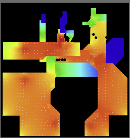
Component and Antenna Placement
After finishing the stackup and fanout, my initial placement for this board is shown below. I’ve included a few polygons for power routing before completing the remaining connections. The initial placement of the 6-pin header was used for programming and reading voltages. The next point to consider is the antenna placement, and finally, we can wrap up with I/O breakouts into our connectors.

In this design, we’ll use a printed antenna to send and receive wireless signals. The best location to place a printed antenna for the nRF52 is along the board edge. This will keep the antenna out of the way of the digital section. The antenna connects to pin E1 on the nRF52840.
If you look at the nRF52 reference design, you’ll see that they provide a printed antenna example that can be incorporated into other designs. This antenna is a quarter-wave antenna, and this can be verified by calculating the length of the antenna and comparing it with the 2.45 GHz signal’s wavelength in a groundless microstrip configuration. The impedance matching network shown in the schematics above should provide sufficient matching given the differences in the stackup for this board.

SWD Programming Header and I/O Header
If you decide to produce this board, you will need to program it. The nRF52840 documentation provides a guide to programming the device through the SWDIO protocol using only 4 pins:
- VDD (system power)
- SWDIO (J2)
- SWDCLK (H2)
- GND
Therefore, I’ve swapped out the 1x6 pin header for an SWD header as this is a standard cable used to program many microcontroller boards (I also have some SWD cables in my lab). Note that the nReset pin (K6) is optional for programming, but I’ll include it in the SWD header pinout alongside a VBAT connection. The finalized pinout on my SWD header is shown below.

The programmer I prefer to use for this type of device is the Forte programmer, which is available from ASIX.net. This programmer supports a long list of devices, including the nRF52840 and some other Nordic products. You’ll have to create custom pinouts for the cable on the Forte, but this is simple enough to do with flying leads.
Next, I decided to swap the initially chosen 1x6 header for a 2x7 header so that I could break out additional I/Os. The header was placed in the top-left corner of the board. I’ve added 22 Ohm series resistors on these I/Os to slow down the signals coming onto the board or leaving the board in case EMI becomes problematic in these interconnects. If it turns out that these are not needed, I can always swap these for 0 Ohm resistors.

Finalized Layout
The finalized PCB layout is shown in the image below. I’ve added some logos, set the part number in the lower-right portion of the board, and aligned the resistors on the I/O lines along the lower half of the pin header. I also did some final cleanup on the silkscreen so that all the designators are clear and there is no overlap. At this point, the design has passed a final DRC and it’s ready to produce.

Source Files and Future Revisions
Although the routing could be improved in a few places just to clean up the I/O access, the board will be functional and I’m happy with how it turned out. Some additional features that could be added include a USB connector and USB charging management IC so that the device could be charged from the standard 5V bus on a USB plug.
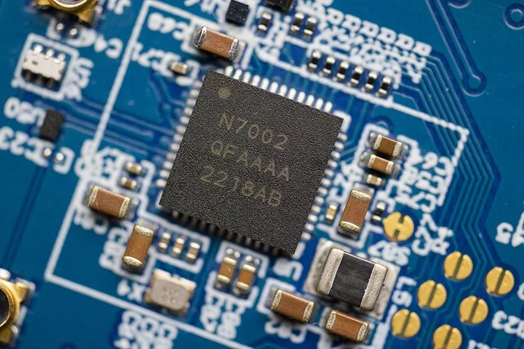
Another component that could be added to the design is a Nordic companion IC that provides WiFi access to nRF52 series MCUs. Last year, in August 2022, Nordic announced the release of its newest iteration of the nRF series: the nRF7002. This SoC offers dual-band WiFi 6 support with ultra-low power consumption as a companion to the nRF52 or nRF53 products. I’ll take a look at this companion IC in an upcoming project and video.
For now, click on this link to download a ZIP archive with the project source files. You can also use the download link in the above embed to access the source files.
High-density components with RF sections are easy to place and route with the complete set of CAD utilities in Altium. When you’ve finished your design, and you want to release files to your manufacturer, Altium makes it easy to collaborate and share your projects.

About Author
Related Resources
Related Technical Documentation
Table of Contents
Design to Release, Without the Friction
- Keep reviews tied to the right version
- Reduce handoff confusion and rework
- Spot sourcing and release risk earlier
- Work solo, share when needed
Get Started
Thank you, you are now subscribed to updates.

