


Support for Rigid-Flex in Altium Designer

At a Glance
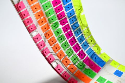
Altium Designer supports flex and rigid-flex circuit design with 3D rendering and the ability to create multiple layer stacks.


Altium Designer's world-class PCB design features help users quickly get started with new rigid-flex designs and prepare them for manufacturing. Rigid-flex in Altium Designer starts with designing a manufacturable PCB layer stack complete with via transitions and any calculated impedance requirements. Flex sections also need to be placed in the layer stack before moving into the PCB layout. Once inside the PCB editor, bending lines can be clearly defined in the PCB layout, and these can be visualized in Altium Designer's 3D PCB design tools. Keep reading to see how Altium Designer supports your flex and rigid-flex designs.
Support for Rigid-flex in Altium Designer
Altium Designer's PCB editor is a layered design environment, supporting up to 32 signal layers and 16 plane layers. These copper layers are separated by insulation layers. In a traditional rigid PCB these insulating layers are typically fabricated using FR4 core and pre-preg, although there is a range of materials available, each with properties that suit different applications. For a traditional rigid PCB these copper and insulating layers exist across the entire PCB, so a single layer stack can be defined for the entire board area.

The layer stack for an eight layer rigid circuit, as it was configured in earlier versions of Altium Designer.
A rigid-flex design does not have a consistent set of layers across the entire circuit design, the rigid section of the board will have a different set of layers from the flexible section. And if the rigid-flex design has a number of rigid sections joined by a number of flex sections, then there may be a different set of layers used in each of these sections. A PCB editor with a single layer stack cannot support this design requirement. To support this, Altium Designer's layer stack management system has been enhanced to support the definition of multiple stacks, as shown below.

The Layer Stack Manager supports the definition of any number of layer stacks.
Multiple Layer Stacks
To support the need to define a different set of layers in different areas of the board design, Altium Designer supports the concept of multiple layer stacks. This is achieved by having an overall master layer stack that defines the total set of layers available to the board designer in this design. From this master layer stack, any number of sub-stacks can be defined, using any of the layers available in the master stack. Each sub-stack is defined and named, ready for use in the rigid-flex design.
The Board Shape
The layer stack defines the board design space in the vertical direction, or Z plane. In Altium Designer, the board space is defined in the X and Y planes by the Board Shape. The board shape is a polygonal region of any shape, with straight or curved edges that lie at any angle, which can also include cutouts (internal holes) of any shape. The board shape is a fundamental concept in Altium Designer's PCB editor, it defines the area available for design - where the components and routing can be placed - and all of Altium Designer's intelligent analysis engines, such as the design rule checker or the autorouter, operate with the boundaries of the board shape.
Note that there is a single, overall board shape for the entire circuit design, including rigid-flex. Within this board shape, any number of board regions can be defined by placing Split Lines to divide the board into separate regions. The image below shows a board shape that has been divided into 3 regions, by the placement of the 2 horizontal blue Split Lines. Use the links above to learn more about splitting a board into multiple regions.

An unusual rigid-flex board shape with two rigid sections and a wrap-around flex ribbon.Note the horizontal dashed blue Split lines; these divide the flex ribbon into 3 separate regions.
Assigning a Layer Stack to a Board Region
In a traditional rigid PCB, the copper and insulating layers exist across the entire PCB, so a single layer stack can be defined for the entire board shape. For a rigid-flex design made up of a number of rigid and flex regions, where each region needs a different layer stack, an alternative approach is needed. In Altium Designer, this is achieved by supporting the ability to assign a layer sub-stack to a specific region of the board shape. To do this, double click on the region to open the Board Region dialog, then select the required Layer stack in the dropdown, as shown in the image below.

Double-click on a region to open the Board Region dialog and assign the required layer stack.
If a region has a layer stack assigned, and that stack has the Flex option enabled, then Bending Lines can be placed across that region. Each Bending Line has a: Radius, Bend Angle and an Affected Area Width property, allowing them to be displayed in their folded state, as they would be in a real-world situation.

Bending Lines have been defined, allowing this rigid-flex board to be displayed in its folded state.
Displaying and Folding a Rigid-Flex Design in 3D
Altium Designer includes a powerful 3D rendering engine for 3D PCB layout, MCAD design tasks, and ECAD/MCAD collaboration. The engine enables presentation of a highly realistic 3 dimensional representation of the loaded circuit board. This engine also supports rigid-flex circuits, and when it is used in combination with the Fold State slider allows the designer to examine their rigid-flex design in the flat state, the fully folded state, and anywhere in between.
To switch to the 3D display mode, press the 3 shortcut key (press 2 to return to 2D, or 1 to return to Board Planning Mode). The board will be displayed in 3D, and if the component footprints include 3D Body Objects that define the mounted component, then these will also be displayed. In the image below you can see that the board includes a battery and a battery clip.
To apply all of the Bending Lines, slide the Fold State slider - it's in the PCB panel when set to Layer Stack Regions mode - as highlighted in the image below. Note that the bends are applied in the order defined by their sequence number. Bending Lines can share the same sequence number, it simply means that those bends will be folded at the same time when the Fold State slider is used. The board can also be folded/unfolded by running the View » Fold/Unfold command (press the 5 shortcut).
You can only fold a board if one of the rigid sections has the 3D Locked checkbox enabled in the Board Region dialog. Altium Designer needs this to know which section of the board must remain fixed during the folding process.

Use the Fold State slider (or the Fold/Unfold command) to apply all Bending Lines in the order defined by their sequence value (Fold Index).
When you're ready to create your next flex or rigid-flex design, use Altium Designer® and its complete set of PCB design and manufacturing features. Once you're ready to release your design data to your manufacturer, you can easily share and collaborate on your designs through the Altium 365™ platform. Everything you need to design and produce advanced electronics can be found in one software package.
We have only scratched the surface of what is possible to do with Altium Designer on Altium 365. Start your free trial of Altium Designer + Altium 365 today.
About Author
Related Resources
Related Technical Documentation
Table of Contents
Design to Release, Without the Friction
- Keep reviews tied to the right version
- Reduce handoff confusion and rework
- Spot sourcing and release risk earlier
- Work solo, share when needed
Get Started
Thank you, you are now subscribed to updates.

