How to Choose the Correct Solder Mask Thickness and Type for Your PCB

When looking at a circuit board, especially as a beginner in the electronics industry, I always wondered why the top layer of PCBs was green. The answer varies depending on who you ask, but one thing everyone agrees on is this: your solder mask aids inspection, provides protection for conductors, and prevents visual fatigue during hand assembly. The various PCB solder mask types differ in how they are applied, their composition, and of course price.
When you are determining the right type and thickness of solder mask you need for your board, you’ll need to consider your manufacturer’s capabilities and your inspection/assembly process. Here are the four PCB solder mask types:
- Liquid epoxy solder mask
- Liquid photoimageable solder mask (LPSM)
- Dry Film Solder Mask (DFSM)
- Top and Bottom-side Masks
What is Solder Mask for PCBs?
Solder mask, also called solder stop mask, is a PCB process used to protect metal elements on a circuit board from oxidation, and to keep conductive bridges from forming between solder pads. It's a critical step in PCB manufacturing, especially if reflow or solder bath is used. These techniques don't provide much control over where molten solder bits land on the board, but your solder mask layer gives you some level of control. Solder mask is sometimes called “solder resist,” which I think is a better term since I used to think that solder mask was a full layer of solder applied to the board.
PCB Solder Mask Types
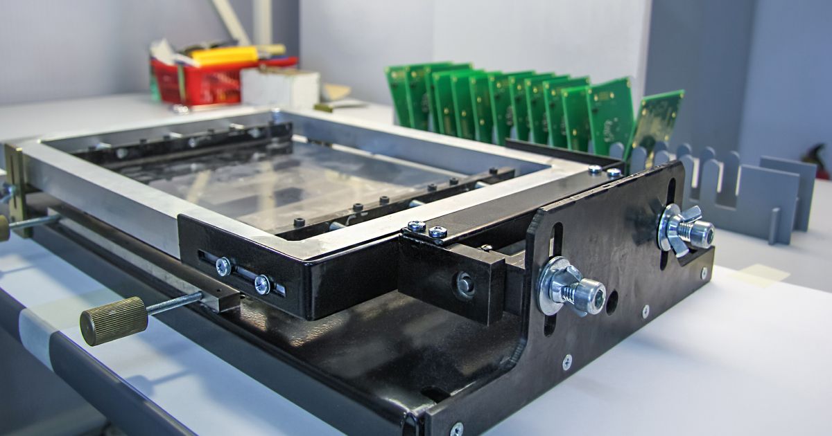
All solder stop mask layers consist of a polymer layer that is applied over the metal traces on a printed circuit board. There are different PCB solder mask types, and the best option for your board depends on cost and your application. The most basic solder stop mask option is to use a silkscreen to print a liquid epoxy over the conductors. This is like airbrushing paint through a stencil. Solder mask can be applied in nearly any color.
Liquid Epoxy Solder Mask
The most basic solder mask option is to use a silkscreen to print a liquid epoxy over the PCB. This is the lowest-cost and most popular solder stop mask option. In this process, a woven mesh is used to support ink-blocking patterns. The epoxy liquid is a thermosetting polymer, which will harden during a thermal curing process. The solder mask dye is mixed into the liquid epoxy and cures to the desired color.
Liquid Photoimageable Solder Mask (LPSM)
Fancier solder masks use a photolithography process with either a dry film or a liquid solder resist, similar to that used for photoresist exposure in semiconductor fabrication. LPSM can be silkscreened like an epoxy, or it can be sprayed over the surface, which is often a cheaper application method. The more advanced (and accurate) method is to use a lithography process to define solder mask openings for pads, vias, and mounting holes.
In this process, a photolithography mask that matches your desired solder mask is made from your Gerber files. Your panelized board is then thoroughly cleaned to ensure no dust particles are trapped under the hardened solder resist. The panels are completely covered on both sides with the liquid LPSM.
One thing you will notice with LPSM is that the black portions of the photolithography mask define areas where you want conductors to be exposed, while areas of the board that you want covered in solder mask will be clear.
Solder masks are applied as an epoxy or a photoimageable polymer.
Once the boards are covered with LPSM, the boards are dried in an oven and placed into a UV developer. The photolithography mask is carefully aligned over the dried board and the board is illuminated with UV light. The exposed areas of LPSM material are cured by the UV light, while the unexposed areas are washed off with a solvent, leaving behind a hard layer of solder mask.
Dry Film Solder Mask (DFSM)
DFSM solder mask is applied using a similar process as LPSM. Both PCB solder stop mask types are exposed in a photolithography-type process. Rather than being applied as a liquid, the dry film is applied in sheets of solder mask film using a vacuum lamination process. This vacuum lamination step forces the unexposed solder resist film to adhere to the board and removes bubbles from the film. After exposure, the unexposed areas of the solder mask are removed with a solvent, and the remaining film is cured in a thermal process.
Top and Bottom-side Masks
If you look at other guides on PCB solder mask types, two types of solder stop mask that are often mentioned are top-side and bottom-side masks. These simply refer to the particular solder mask placed on either the top or bottom sides of the board; they do not refer to a particular fabrication process or specific type of solder mask material.
The Final Steps: Curing and Surface Finish
Applying the media shown above requires the boards be cleaned to remove any dust. Afterwards, they too will go through their final hardening and curing processes. The liquid epoxy solder mask is cured thermally as there is no UV exposure. LPSM and DFSM films are cured by UV exposure during the photolithography process. After exposure, these films are cured and hardened with a heat treatment.
No matter which of the PCB solder resist types you use, the resulting solder mask will leave exposed areas of copper on the board. These exposed areas must be plated with a surface finish to prevent oxidation. The most common surface finish is hot air solder leveling (HASL), although other popular surface finishes are electroless nickel immersion gold (ENIG) and electroless nickel electroless palladium immersion gold (ENEPIG). Additional holes in the mask layer are left for the paste mask when applicable. The paste mask is used to attach pads or other components to the printed circuit board, and is done differently depending on various manufacturing processes.
ENIG plating on exposed copper through a solder mask.
What is the Standard Solder Stop Mask Thickness?
The thickness of your solder stop mask primarily depends on how thick the copper traces on your circuit board. LPSM and DPSM solder mask thickness in empty areas of the board will generally vary with location. The typical solder resist thickness (perpendicular to the board) is at least 0.8 mils. Solder mask will be thinner near the edges of traces and can reach as thin as 0.3 mils or less. In general, you’ll want about 0.5 mils of solder mask over your traces. Sprayed epoxy solder mask can take a more uniform thickness throughout your PCB.
In addition to preventing corrosion on copper traces, solder stop mask is used to place a dam between neighboring pads on a circuit board. For component pads, this is done by defining a small gap between the solder mask and exposed pads, called a solder mask relief. This creates a dam that prevents molten solder on one pad from flowing onto a neighboring pad. This is especially important in fine-pitch BGAs and other components with high pin density. This small relief around the edge of a pad allows the solder droplet to sufficiently wet the pad and hold itself in place, which prevents bridging during soldering. You can read more about using solder resist relief on a circuit board to prevent SMT process defects in this article.
You can’t see it from far away, but a small solder mask relief is placed around the pads for the central IC.
What Color Should Solder Mask Be?
The color of your solder mask is determined by the dye used in the solder mask material, and the chemical properties of the dye will influence the cured solder mask thickness. One reason that green solder stop mask is extensively used is that it can be used to create thin solder mask dams (~0.1 mm). The dyes used in solder masks with different colors tend to form thicker solder mask dams. No matter which dye you choose to use, solder resist thickness on PCBs for use in certain industries or applications is defined in IPC-SM-840D.
The solder stop mask color is an important part of automated or manual visual inspection. Black solder mask provides the lowest contrast between the board and traces, which can create difficulty in automated inspection. This is another reason green masks are preferred. The silkscreen color you use will also influence visual contrast and will influence visual fatigue during manual inspection.

The traces beneath this black solder mask can be very difficult to see.
Like any other fabrication parameter or process, you should consider how sensitive your final application will be, and plan your design accordingly. It's always important to discuss the fabrication options with your manufacturer. They may even be able to suggest better options based on their capabilities.
What Solder Mask Should I Use?
Deciding on an appropriate solder mask depends on the physical dimensions of your board, holes, components, and conductors, the surface layout, and the final application for your product.
First, if you have a PCB solder resist that will be used in aerospace, telecom, medical, or other “high reliability” industries, check on industry standards around solder mask, and your intended application in general. There are specific requirements that supersede whatever else you learn on the internet.
For most modern printed board designs, you’ll want a photoimageable solder resist. The surface topography will dictate whether to use a liquid or dry application. A dry application lays down a uniform solder mask thickness across the entire surface. However, dry mask adheres best if your board surface is very flat. If you have complex surface features, then you’re probably better off with a liquid (LPSM) option for better contact with the copper of your traces and the laminate. The downside to a liquid application is that the thickness isn’t perfectly uniform across the board.
You can also get different finishes on the mask layer. Talk to your manufacturer about what they have available and how it will affect production. For example, a matte finish reduces solder balls if you are using a solder reflow process.

PCBs manufactured using a solder reflow process need a solder mask. The finish of the mask can affect the quality of the reflow.
How Do I Include Solder Mask in my PCB Layout?
When you design your printed circuit board, the solder stop mask should be its own layers (top and bottom) in your PCB layout and your Gerber files. This won’t be defined in your layer stack manager. Instead, it is usually defined as an additional layer by default in your CAD tools. You'll typically want a 2 mil border around your feature in case the solder mask isn't perfectly centered. You'll also have a minimum distance between pads, often 8 mils, to ensure the mask can prevent solder bridges from forming.
If you're in the business of designing or producing PCBs, it’s important to choose PCB design software that lets you select different PCB solder resist types. Altium gives you access to a complete set of PCB layout and manufacturing tools, and it gives you control over every aspect of your designs.


