Mouse Bites and V-Scores: How to Depanelize PCBs

At a Glance
If you build your own PCB panels, there are two simple ways to detach PCBAs. These are mouse bites and V-scores. Here is how to design these into a PCB panel.


Most designers don't build their own panels, unless they grab a template from a PCB manufacturer and fill in the details by hand. In Altium, there is a tool that will allow you to arrange boards into a panel, called the Embedded Board Array. You could use this to estimate the number of boards per panel in a production run, or to design your own panel for hand assembly.
If you want to build your own panel and detach boards yourself, you will need some way to cut the boards from the panel prior to assembly. To do this, we can add two possible features into a panel: V-score grooves and mouse bites. When these are added to a panel, it will be much easier for a designer to break boards apart by hand rather than routing them out from a panel.
How to Design Mouse Bites
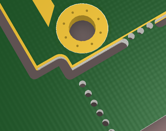
Mouse bites are designed by placing cut-out regions and holes between the boards in a panel, which leaves behind small tabs connecting the boards in a panel. With these small tabs connecting PCBs, the fabrication house could ship an etched panel to a designer or assembler, and the PCBs can be detached by hand before assembly. The leftover material can be filed away by hand or it can be trimmed away with a router.
The drill holes are sized and spaced such that there is a small amount of material between the breakaway tabs and a PCB. This allows a designer to break the guide tabs around the edges and then break the boards apart by hand. Mouse bites in a PCB layout look like the arrangement shown below.
Many fabricators will place Mouse bites for you if you do not specify V-score or panel routing.
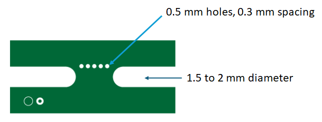
There are five important points to note when placing holes for mouse bites along a board edge:
- Place holes tangent to the PCB edge
- Hole diameter should be reasonably large
- Hole-wall spacing should be smaller than hole diameter
- Routing area around the holes is typically 1.5 mm to 2 mm
- Indicate routing tool diameter and routing path in a fabrication drawing
The image below shows some example dimensions of the routing and hole arrangement. The boards are routed right up to the region with the holes, and that routing space has been cleared of any PCB laminate material. The remaining area is the rest of the breakaway tab attachment and the holes. The hole sizing below is just an example from, some fabricators will have their own requests or requirements for routing and hole size.
By placing the holes tangent to the board edge, there will be minimal intrusion into the board region. If you plan to use mouse bites in your design, then there needs to be enough board edge clearance, both for copper and components. When the holes intrude into the board Edge you may risk exposing any internal copper through the side of the board.
When mouse bites are detached, they leave small bits of PCB material left over, which usually need to be filed off to create a clean edge. This motivates an alternative method to remove PCBs from a panel: V-scoring.
How to Design V-Score Grooves
V-score grooves in a PCB panel are small groves where some material has been cut away, which defines a narrow cut line for depanelization. Removal of PCBs with V-scoring basically involves the use of a rolling blade to cut PCBs from the panel along the V-scored groove. V-scoring can also provide a sufficiently flexible groove such that PCBs could be broken apart by hand. It can also be used with a batch of PCBs in the same assembly, thus a larger board could be broken into smaller PCBs as needed; I have used this to create PCB samples for clients.
V-scoring does not require placement of any cutouts or holes in the PCB panel. However, if you want to use V-scoring, you should make sure to indicate the score locations in a mechanical layer.
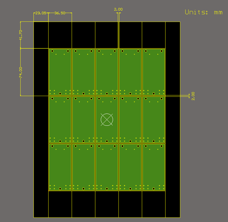
Example mechanical layer in an embedded board array. The yellow grid lines show V-score paths.
With this mechanical layer, you could export the layer to a DXF file and use it in a panel drawing, or you could export it as one of the Gerber layers for your panel.
There are some important design rules for scoring in a PCB panel. The reason we have these rules is due to the clearances required around the score region and the flexibility of the PCB near the score.
- Apply a large clearance between the score region and nearby copper in each PCB.
- If no leftover material is desired, panel the PCBs right next to each other but increase the board outline clearance in the PCB.
- Avoid placing components very close to the score region.
- Mounting holes, silkscreen, etc. may note require the same large clearances as copper.
Once the V-score locations are determined, the locations need to be indicated on a PCB panel drawing. The V-score groove detail also needs to be indicated with a dimensioned drawing, such as in the example shown below. This example indicates the desired score angle and depth into the surface of the PCB, as well as the remaining material between the grooves on each side of the panel.
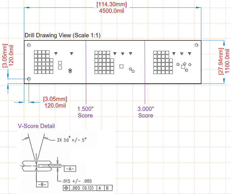
V-score locations and detail in Draftsman.
Other Tasks
Panel design doesn’t end with adding mouse bites, V-score grooves, or routing paths for detaching PCBs. There are other tasks required when creating the PcbDoc file for your panel:
- Verify that your fabrication house stocks materials in your panel size matching your PCB stackup
- Add tooling holes and fiducials to the corners of the panel, and make sure the required number of tooling holes is included
- Add any test coupons/structures for controlled impedance testing to the panel if required
Once the panel is finished in a PcbDoc file, you can use an OutJob file to export the Gerbers for the panel and send these to your fabrication house. You can also export a fab drawing of the panel and use it in a custom panel drawing, or you can create a panel fabrication drawing in Draftsman.
Whether you need to build reliable power electronics or advanced digital systems, use the complete set of PCB design features and world-class CAD tools in Altium. To implement collaboration in today’s cross-disciplinary environment, innovative companies are using Altium to easily share design data and put projects into manufacturing.

About Author
Related Resources


Related Technical Documentation

Thank you, you are now subscribed to updates.


