Ready to Scale? Time to Optimize Your PCB Design

At a Glance
Implement PCB cost optimization, ensure PCB quality control, and reduce PCB cost with these strategies for scaling PCB manufacturing.


I received an excellent question on my LinkedIn recently, and this relates to how designers and procurement heads have to work together to prepare a design for scaling. Pre-production review and scaling into volume production involve many dimensions of design testing, evaluation, and modification. Assuming everything in the design has passed review and no more prototype spins are needed, you can then look to optimize and design for cost, performance, size, EMI, thermal, and probably many other areas.
Turn Up the Volume
The first question you should probably ask yourself regarding volume production is very simple: what is your expected production volume?
I'm surprised how many times I get into a contract design only to find out that the client has not determined what their expected production volume is. I understand that it sometimes depends on sales numbers, but a reasonable estimate is always helpful. This will be important if we start looking at cost discounts on certain components, potential parts swaps based on performance and reliability, or design changes required to comply with reliability standards.
Some of the biggest areas for cost reduction when purchasing at volume are found below. The big challenge when producing at volume is to address these areas without sacrificing production yield, quality, and reliability.
|
PCB material composition |
|
|
Component selection |
|
|
Mechanical elements |
|
|
Bare board features |
|
|
Quality control |
|
This list shows common areas where you might be asked to cut costs in order to meet a budget or make a product's pricing more competitive. But the challenge in the above cases is to prevent quality problems and ensure reliability. When producing at volume, it is often the case that we look for a lowest-priced technically acceptable (LPTA) solution. Now let's dig into some simple examples that illustrate how we can prepare for volume production.
Part Number Consolidation
This should be the most obvious place to start reducing cost while possibly improving the reliability and quality of the end product. Consolidating part numbers means using a single part number throughout the bill to the largest extent possible. Doing this correctly can involve putting passives in series or parallel to reach target design values, using one type of pin header, etc. Doing this gives you access to volume discounts on components, and those savings can add up quickly when you look at some components like discreet semiconductors and connectors.
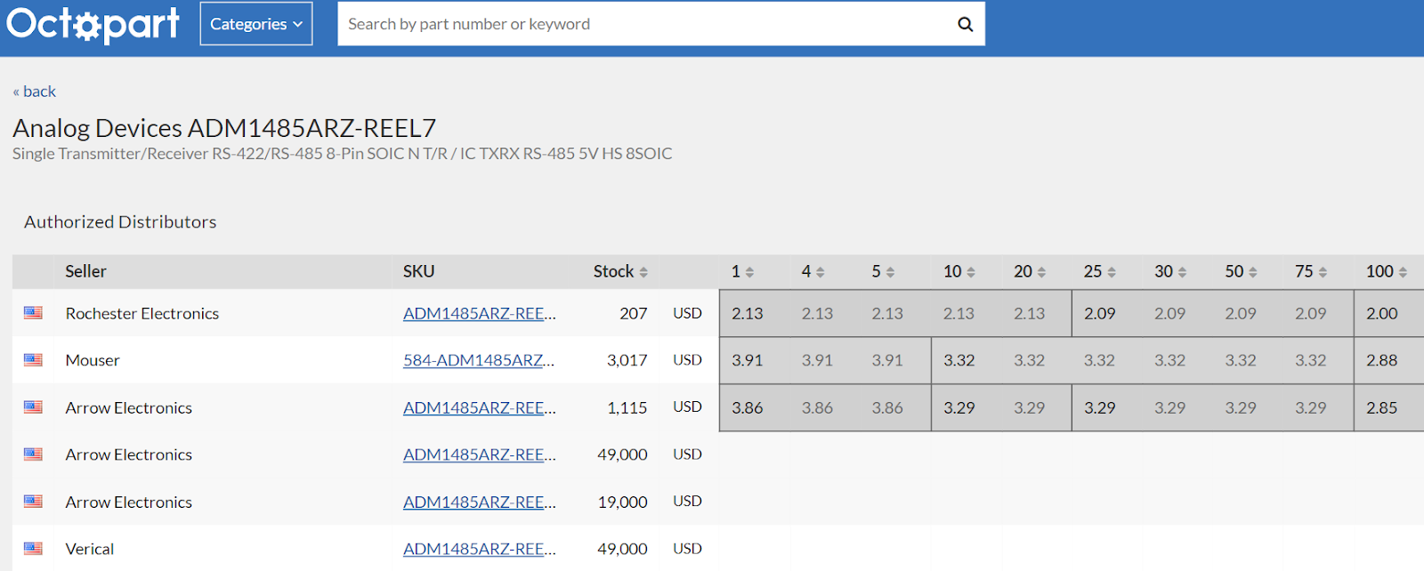
Octopart’s database shows price breaks for volume purchases across the entire supply chain.
Part Package Consolidation
When finalizing the board, you can get further quantity discounts without compromising reliability by consolidating down to a single package size, especially for passives. It's common to see mixed package sizes on a pcb, and this is usually done for power rating purposes. But if you know that certain parts do not require such a high power rating, you could change passives with common values to smaller packages. This could get you over the next hump of volume discounts, and it requires minimal changes to the PCB layout.
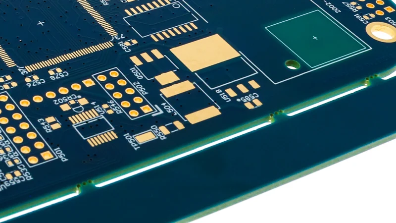
PCB Materials
The materials in your PCB always incur some cost, but they will be the major determinant of performance and reliability. If your board doesn't require an advanced FR4 laminate, high TG material, high CTI material, or PTFE then don't specify it in your build. Think about the end operating environment in which the board will exist before selecting more expensive materials for the stack up.
The same applies to surface finishes. The moment you add a precious metal into your surface finish you will see a cost increase. If this is not needed for performance or reliability, then stick with ImSn, HASL, or Sn-Pb alloy plating.
Gold-based platings in a PCB greatly increase costs but are highly preferable for reliability.
Surface coatings and additional materials like conformal coatings also add cost. They could be a big determinant of reliability or functionality, so be careful before swapping to a lower cost material or eliminating a material. Keep your material selection within the LPTA philosophy if cost is a major competitive factor for your product.
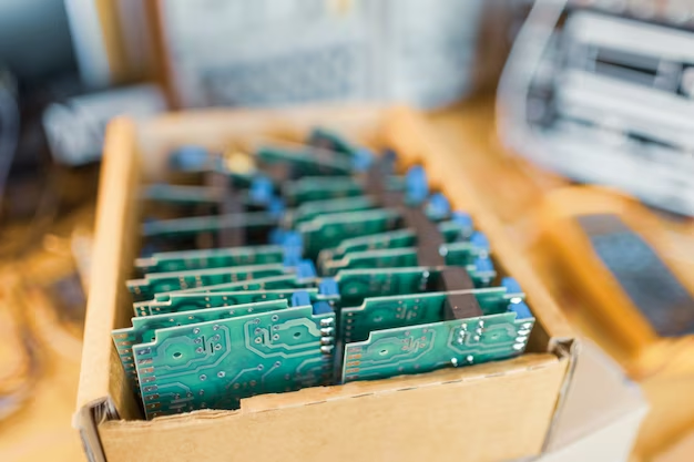
Bare Board Features
During production, each board will go through many inspections and tests to ensure it was fabricated correctly. But before taking a board to production, it’s your responsibility to test multiple prototypes in order to identify any defects in the board that tend to arise repeatedly. Your team will need to address these thoroughly as part of pre-production planning.
If your contract manufacturer’s quality team starts to notice repeated defects, they will come back and tell you about these defects so that the design can be improved. It's hard to generalize what the most common defects are for any build, but some of these common defects might include:
- Insufficient solder or too much solder
- Bridging across pads
- Solder mask sliver snapping off
- Bridging or shorts internally in the PCB
- Poor connections to pads (tombstoning, head-in-pillow, etc.)
At some point, I've seen every one of the defects on this list. The instances where I have experienced these are when board features become too aggressive for capabilities or when a land pattern is not designed correctly for the component pin pitch (or both). The simplest approach here is to look at board feature limits in your manufacturer's capabilities, and apply a margin of safety; this can address many of the simpler quality problems found in assembly.

Internal NFPs with low pad-to-plane clearance could create a chance of a short.
Part Swaps
At some point along your prototype testing, you may have identified some parts swaps that are necessary to ensure reliability. I think the most common of these is the need to increase the temperature limit for certain parts, which is definitely something I have experienced.
Another area where there are parts swap opportunities is in the precision level for certain components like passives. Some passives need to have very high precision values, such as when they are being used for precision measurements and their values are part of a calculation. Probably the most common example is with precision measurements in an ADC.
If you have a bunch of 1% precision part numbers in the board where you don't need them, swap them out for 5% or looser tolerance components. This will also reduce costs. As long as it's on the right parts, you won't see any effect on reliability.
Production Planning
Everything above focuses on the PCB and PCBA, but there is still a lot more that goes into the full production of an electronic device and not just the PCBs. Product manufacturing often requires contracting with a manufacturer for the enclosure, wires and cabling, connectors, and even the product packaging; there is no facility that does it all. Not all PCB manufacturers will assist with this, instead you will have another manufacturer you will have to work with in order to complete these tasks.
There's also the matter of logistics. Someone has to take charge of coordinating delivery of all these different materials and parts. Companies that are scaling for the first time may even need to implement their own internal quality control measures on the finished product, and there is some logistical effort for that as well.
When a company decides to take a product to market, there will be a lot of pre-production planning that spans beyond the PCBs/PCBAs. Take a look at all of the areas mentioned above with your team, including the logistical aspects. Decide what will remain in-house and what will be contracted out. This can even include production or assembly of custom components like bespoke transformers and connectors. A bit of planning early on streamlines this whole process and helps you get to market quickly with high-quality products.
Whether your team is creating advanced prototypes or transitioning a new product into manufacturing, Altium Designer® gives PCB designers everything they need to design for cost and quality. When you’re ready to share your outputs with your manufacturing house, you can use the Altium 365™ platform to collaborate across design and production.
We have only scratched the surface of what’s possible with Altium Designer on Altium 365. Start your free trial of Altium Designer + Altium 365 today.

About Author
Related Resources


Related Technical Documentation

Thank you, you are now subscribed to updates.


