


How Thermoformed Flex PCB’s are Designed and Fabricated

At a Glance
In today’s fast-paced world of electronics, we’re always on the lookout for components that are more compact, durable, and flexible to add to the toolbox. Flexible materials and flexible circuit technology continues to be a winning solution.


Flexible circuits continue to be a winning solution when durability and compact form factor are required. The obvious benefits of being thinner and lighter weight with the ability to be flexed and folded are easy to understand and the technology has been in use for decades.
While we often spend time looking at materials, how to design for flexibility, and understanding the fabrication process, today we are going to specifically look at thermoformed flexible printed circuit boards. This technology is particularly interesting because the circuits can be molded into specific shapes while maintaining their performance. As with the more traditional applications for flexible materials, thermoforming is not a new technology, but it does add another layer of complexity to both the circuit design and the fabrication process.
Circuit Design Considerations
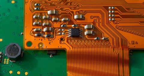
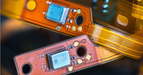
Thermoformed flex PCBs are a special kind of flexible printed circuit board that can be permanently shaped during manufacturing. Flex PCBs can be mechanically bent into a desired static bend radius, as Zach Peterson discusses in this linked article. Unlike the usual flex PCBs that just bend and flex, or that are mechanically fixed after fabrication, thermoformed flex PCBs are molded into fixed shapes.
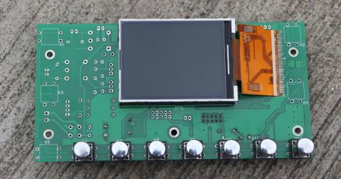
They are typically designed in places where space is tight and you need precise shapes, like in cars, medical devices, and wearables. If you consider applications such as your car’s dashboard or the latest wearable health monitor, thermoformed flex PCBs make these sleek designs possible by fitting into compact spaces and conforming to complex shapes.
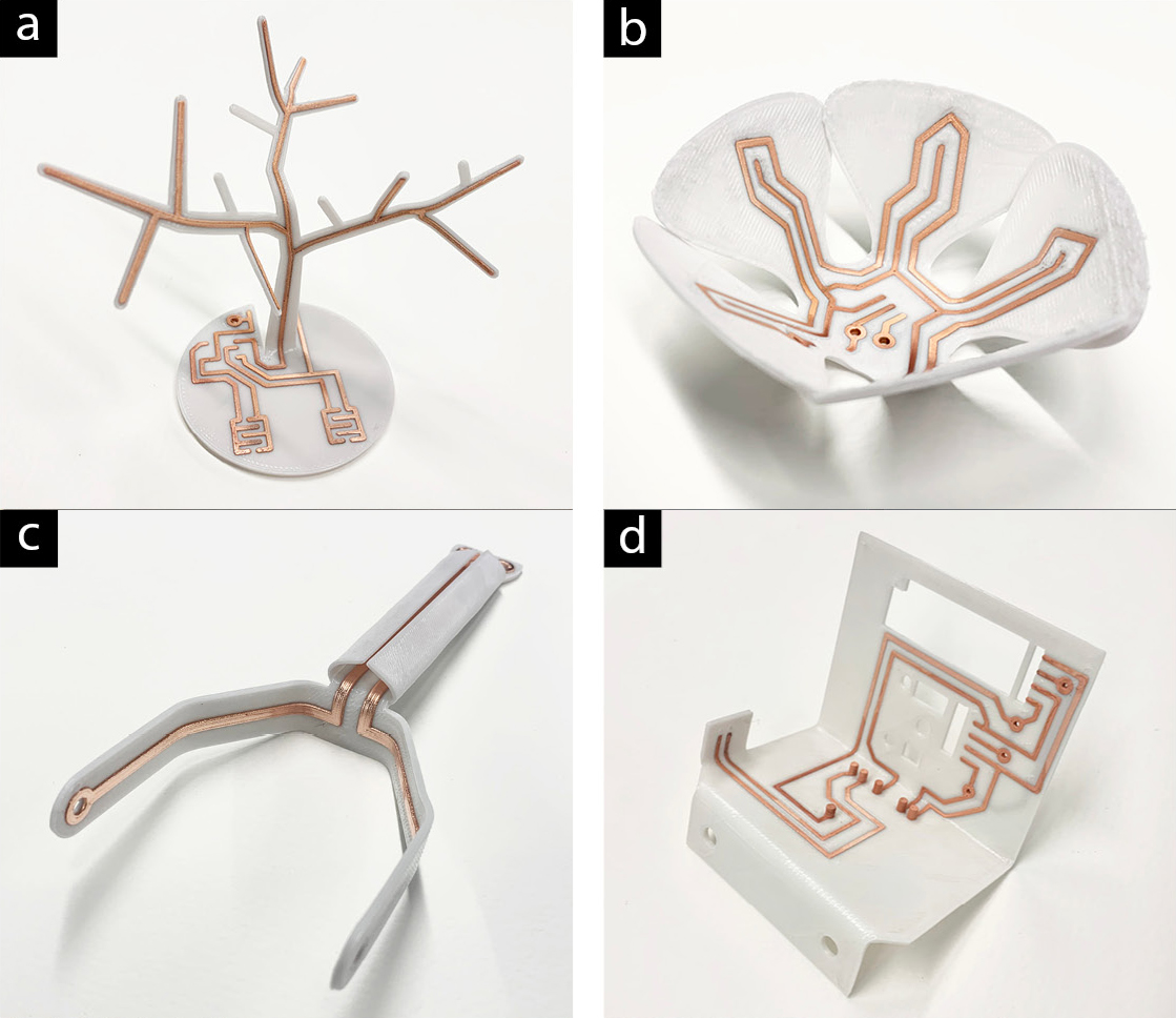
Thermoformed flex PCB example images from FreddieHong19 on github
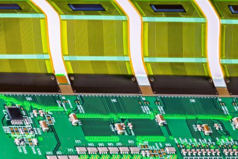
When it comes to mechanical design, you need to think about how the PCB will bend and flex, both during the forming process and in its final use. Avoid putting traces and components in high-stress areas. Using curved traces and staggered vias can help spread out the stress and reduce the risk of cracks. These are very similar to molded interconnect devices (MIDs), but the main difference is that thermoformed PCBs have their bending applied after fabrication is completed.
While it seems like thermoformed flex technology would be a fantastic solution in any number of applications, it is also a difficult technology to fabricate and subsequently to design. There are many factors to consider to ensure a successful outcome.
Fabrication Process For Thermoformed Flex PCBs
The fabrication process for thermoformed flex PCBs involves several precise steps to achieve the desired shape and functionality and I think it is important to point out that thermoforming is not a “standard” or even typical capability for most flexible circuit manufacturers. It requires strict process control and another level of process capabilities.
Polyimide and polyester (e.g., polyethylene terephthalate) are popular material choices because they’re flexible and can handle heat thanks to their high decomposition temperatures and high glass transition temperatures. Polyimide is a favorite because it can withstand high temperatures during the thermoforming process, and processing is well understood by many fabrication houses.
Thermoforming Tooling: The creation of the 2D version of the flexible circuit is as you would expect for any flexible circuit fabrication process. Once the circuit pattern is created and has passed quality review, the thermoforming takes place.
Before any heating begins, the mold used for shaping the PCB must be prepared. This mold is typically made from materials that can withstand high temperatures without deforming, such as metal or heat-resistant plastics/polymers. The mold must be precisely machined to the exact dimensions and shape required for the final PCB design. One new approach for thermoforming is to use 3D printed molds; see for example the below molds from Proto3000:
Proto3000 3D printed thermoforming molds. (Image source)
Fixation and Heating: The flexible PCB substrate, which has already been patterned and plated, is carefully placed into the mold. Proper alignment is crucial to ensure that the PCB conforms to the desired shape without any misalignments or distortions. This step often involves using specifically designed alignment tools or fixtures to keep the PCB in place during the heating process.
The heating stage and process control is critical. The entire assembly is heated to a specific temperature where the substrate becomes pliable. This temperature must be precisely controlled to avoid overheating, which can damage the material or the conductive traces. The heating can be done using various methods, including convection ovens, infrared heaters, or specialized thermoforming equipment. The key is to apply heat evenly across the PCB to ensure uniform pliability.
Once the substrate reaches the required temperature, it becomes soft and pliable. The mold then shapes the PCB into the desired three-dimensional form. This step must be done quickly yet carefully to ensure that the PCB conforms to the mold without introducing any wrinkles, bubbles, or other defects. The pressure applied during forming must be evenly distributed to avoid stressing the material.
As an example, DuPont provides thermoforming guidance for their Kapton line of materials, including fixturing and pressing time/temperature values based on the depth of the forming mold. Read their guidelines for Kapton films here.
Cooling and Solidification: After the PCB has been shaped, it needs to be specifically cooled down to solidify its new form. Cooling must be controlled to avoid introducing internal stresses or defects like warping and cracking. Cooling too quickly or not quickly enough can lead to defects in the final design. The cooling process can be managed using controlled air cooling, water baths, or integrated cooling systems within the thermoforming equipment. Gradual and even cooling is necessary to maintain the integrity of the PCB.
Removing the flexible circuit from the mold also requires great care. After the PCB is removed from the mold, it undergoes another thorough inspection and quality control checks. This includes visual inspections for surface defects, dimensional checks to ensure the PCB conforms to the desired shape, and mechanical tests to assess the structural integrity.
Advanced Processes in Thermoformed Flex PCBs
The field of flex PCBs in general is evolving, with new advancements and innovations on the horizon. Research is ongoing to develop new materials with enhanced properties, such as increased flexibility, better thermal stability, and improved electrical performance. These advancements will expand the potential applications of thermoformed flex PCBs and improve their reliability.
Higher density fabrication technologies, such as laser direct structuring (LDS) and additive manufacturing processes (mSAP or SAP), can bring high density interconnect (HDI) design approaches into flex PCBs, which could then also be used in thermoformed devices. These techniques offer higher precision, greater flexibility in design, and reduced production times.
The thermoforming process is a delicate balance of precise temperature control, careful handling, and rigorous quality assurance. Each step, from heating to cooling, must be meticulously managed to produce high-quality thermoformed flex PCBs that can withstand the demands of their intended applications. If you are considering a thermoformed flexible circuit for your application, work with your fabricator early in the design process to ensure the highest level of success.
About Author
Related Resources
Related Technical Documentation
Table of Contents
Design to Release, Without the Friction
- Keep reviews tied to the right version
- Reduce handoff confusion and rework
- Spot sourcing and release risk earlier
- Work solo, share when needed
Get Started
Thank you, you are now subscribed to updates.

