


Increase Your Component and Trace High Density With Via-in-Pad Plated Over Technology

At a Glance
Via-in-pad technology is critical in HDI designs. These tips will help you increase routing density and work with fine pitch components using via-in-pad designs.


When components get packed too close together and all the routing moves to the inner layers, the required via type often shifts to via-in-pad. The use of via-in-pad enables higher component density by removing the space normally reserved for nearby vias. This also tends to push more routing into the inner layers, especially once fanout channels disappear around fine-pitch components.
We tend to see a few design practices used together, which collectively end up forcing the use of via-in-pad. Close component placement, smaller packages, and finer-pitch BGAs all push designers into via-in-pad, ultimately requiring plating over the via holes when component placement exists on both sides of the board.
So if you are wondering when it is appropriate to use via-in-pad plated over, this guide will help you make the right design decisions. Via-in-pad is not automatically required with more advanced via technologies like blind microvias, but it is often the first step designers take when increasing component density in the PCB layout.
What Is Via-in-Pad Plated Over (VIPPO)?
Via-in-pad is used on SMD components to make space available nearby for other parts, and it is used in situations where placement is quite aggressive. The via is placed directly in the SMD pad, and these vias can be through-hole vias, mechanically drilled blind vias, or microvias.

Blind microvia-in-pad will require fill, cap, and planarization in order to prevent soldering defects in this fine-pitch BGA.
On double-sided PCBs, via-in-pad is often plated over because an open via barrel inside an SMD pad can wick solder during reflow and create a depressed or starved solder joint on one or both sides of the board. When the via is filled, capped, and planarized, the pad behaves much more like a normal SMD pad, which improves solder joint consistency and makes the board more manufacturable when both outer layers contain mounted components.
Certain package types drive via-in-pad much more often than others because the routing channels disappear quickly or because the package includes a large central pad that needs both thermal and electrical access. In dense layouts, via-in-pad becomes less of a convenience feature and more of a routing requirement.
|
Component Type |
Typical Reason for Via-in-Pad |
Common VIPPO Need |
|
Coarse-pitch BGAs |
Escape routing without consuming adjacent channel space |
Sometimes |
|
Fine-pitch BGAs |
Routing density and limited fanout space |
Often |
|
LGAs |
Dense pad fields and limited routing access |
Often |
|
ICs with thermal pads |
Thermal transfer and ground connection through exposed pad |
Common in exposed pads |
|
QFNs |
Ground/thermal vias in the center pad and tight routing nearby |
Common |
|
Leaded packages |
Occasional density relief in very tight layouts |
Less common |
Via-in-Pad Plated Over Process
When designers specify via-in-pad plated over, the fabricator is not simply drilling a via and covering it with copper. A true VIPPO process usually requires filling the via, curing the fill material, capping the via with copper, and planarizing the pad so it can function as a reliable assembly land. The exact sequence varies by fabricator and via structure, but the general process is fairly consistent when epoxy filling is required.
- Drill the via in the required pad location, whether that is a through-hole via or blind via.
- Plate the via barrel with copper as part of the normal through-hole or blind-via plating sequence.
- Clean and prepare the via so the fill material can properly bond inside the hole.
- Fill the via with epoxy or another approved non-conductive fill material.
- Cure the fill material under the fabricator’s controlled process conditions.
- Cap the filled via with copper so the outer pad surface becomes continuous.
- Planarize the surface to remove excess copper or filler and restore a flat pad.
- Apply final surface finish so the SMD pad is ready for soldering.
Specifying Via-in-Pad
When placing a manufacturing order that includes via-in-pad, failing to specify it on the quote form and in the fabrication notes often leads to an email from the fabrication company. The fabricator will ask how the via-in-pad should be handled, because there are multiple possible treatments and they do not all produce the same result. Some vias may be left untented, some may be tented, some may be filled and capped from one side only, and some may be filled and capped from both sides. It is also possible to have unfilled vias that are capped on one side or both sides, although this is not interchangeable with a filled VIPPO structure and should not be assumed equivalent for assembly reliability.
A good fabrication package should identify the required via structure clearly. Common options include:
- Untented
- Tented
- Filled and capped, one side
- Filled and capped, both sides
- Unfilled and capped, one side
- Unfilled and capped, both sides
The required via-in-pad type should be stated directly in the fabrication notes, and it is best practice to reference the applicable IPC-4761 via protection type so the requirement is not left to interpretation. This matters because terms like “filled,” “plugged,” “capped,” and “plated over” are often used loosely in casual discussion, but a fabricator needs an unambiguous instruction set. An example fabrication note entry would be:
|
ALL VIA-IN-PAD LOCATIONS INDICATED IN THIS DESIGN SHALL BE FILLED AND CAPPED IN ACCORDANCE WITH IPC-4761 TYPE VII UNLESS OTHERWISE NOTED. |
Selective Via-in-Pad
Via-in-pad does not always need to be applied across the entire PCB. In many designs, only a few areas actually require it, such as a fine-pitch BGA, an LGA with dense routing, or an exposed thermal pad under a power device. In these cases, selective via-in-pad is usually the better choice because it controls fabrication cost while still solving the routing or assembly problem in the places that actually need it.
Selective application has to be documented carefully because many fabricators prefer to process via fill and cap requirements globally when possible. If the requirement only applies in specific areas, it can be called out with an annotated fabrication drawing, a fabrication note tied to named component locations, a note specifying that only vias inside SMD pads receive fill and cap treatment, or Gerber and fabrication outputs that explicitly identify the fill-and-cap locations. The point is to remove any guesswork before tooling begins.
Planarization
When a via-in-pad is plated over, planarization is the step that restores a flat and solderable surface on the SMD pad. After the via is filled and copper capped, the pad surface may still contain excess material, local height variation, or slight dimpling. Planarization removes those surface variations so the finished land is close to the same geometry a component pad would have if no via existed at all.
This matters because soldering defects often begin with pad surface irregularity. If the plated-over via is not sufficiently planar, solder paste volume becomes less predictable and wetting can become uneven. That is especially problematic in leadless packages and fine-pitch BGAs, where solder volume is already tightly constrained and the joint geometry depends heavily on pad flatness. A non-planar pad can contribute to head-in-pillow risk, voiding behavior changes, insufficient collapse, or inconsistent joint formation across an array.
Planarization is performed after filling and capping by mechanically or chemically reducing the surface until the capped via area blends into the surrounding pad. Fabricators then qualify the result using their internal process controls, cross-sections, surface inspection, and flatness acceptance criteria tied to assembly yield requirements. Typical checks focus on whether the cap remains intact, whether the filler is stable, and whether the final pad surface is flat enough to support consistent solder paste printing and reflow.
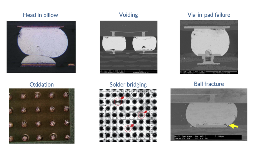
A set of BGA soldering defects; all of these except oxidation are best identified with X-ray inspection. From the webinar: Reduce PCB Assembly Defects With Smart Package Selection
Via-in-pad is a useful density and routing tool, but it should be applied deliberately rather than automatically. VIPPO is most often needed on double-sided PCBs where open pad vias can interfere with soldering on either side of the board. It is generally not required for blind vias or blind microvias used appropriately in HDI structures, since those via types can often avoid the solder-wicking problem that makes filled and plated-over through-hole via-in-pad necessary in the first place.
Whether you need to build reliable power electronics or advanced digital systems, use Altium’s complete set of PCB design features and world-class CAD tools. Altium provides the world’s premier electronic product development platform, complete with the industry’s best PCB design tools and cross-disciplinary collaboration features for advanced design teams. Contact an expert at Altium today!
Frequently Asked Questions
Do most PCB fabrication companies support via-in-pad plated-over (VIPPO)?
Yes. Most PCB fabrication companies can accommodate via-in-pad designs. The ability to fill and plate vias is seen as a standard capability. This is the case in the United States, China, and Europe.
Are special PCB manufacturing outputs needed to specify via-in-pad?
Special outputs are not a requirement to specify the need for via-in-pad and fill/cap processing. At minimum, you can use a fabrication note. The manufacturer will notice that you are using via-in-pad when they examine your drill data against the paste mask layer in your Gerbers; drill hits inside paste mask apertures normally indicate via-in-pad.
Can I use via-in-pad with any type of via?
Yes. You can use via-in-pad with any type of via (mechanically drilled blind vias, laser drilled blind microvias, or through-hole vias). Blind microvias will require full plating to fill the via so that it fully closes. Through-hole vias do not require fill/cap but it is recommended to prevent unnecessary solder wicking.
Is via-in-pad reliable?
Yes, via-in-pad processing produces structures that are widely viewed as reliable. When used in leadless parts like QFNs or BGAs, these vias tend to be very small and may experience reliability problems under thermal cycling, particularly for blind microvias. Design teams should do their own reliability assessments for their products in the field before allowing via-in-pad in manufactured products.
Does Altium support via-in-pad usage?
Yes. Altium allows users to use via-in-pad as a standard feature. Make sure to enable the “Vias Under SMD” rule in the PCB Rules and Constraints Editor. Read the Altium Designer Documentation to learn more.

About Author
Related Resources
Related Technical Documentation
Table of Contents
Design to Release, Without the Friction
- Keep reviews tied to the right version
- Reduce handoff confusion and rework
- Spot sourcing and release risk earlier
- Work solo, share when needed
Get Started
Thank you, you are now subscribed to updates.

