


ISO 14443 NFC Reader Project With ESP32

At a Glance
Access Altium project files for the TRF7970A NFC reader and ESP32 microcontroller PCB design.


NFC readers are simple devices that can be built with small form factor and used in a variety of applications. There are also multiple standards that can be used to design NFC readers, with the most common standard being the ISO 14443 standard. This project looks at implementation of an ISO 14443 standard NFC reader using a Texas Instruments transceiver chip and an ESP32 microcontroller.
As ESP32 is a popular microcontroller, we also opted to provide firmware for the embedded application for this device. The firmware follows a simple process which triggers a relay, which is a typical use case for NFC devices that need to open locks, drive motors, or trigger another device. The Altium project files and firmware can be downloaded from the link below.
Which NFC Reader Standard Should You Use?
The term NFC refers to near-field communication, a short-range communication approach for which there are several standards. Applications of NFC include contactless payments, object sensing, object differentiation, and sending short bursts of data privately. For object detection, the system will interact with an NFC tag device, and the role of the reader is to sense the location of the tag. For an NFC reader, the device operates by emitting a high-frequency magnetic field, and the tag is sensed by interacting with an NFC coil or antenna. The tag and the reader coil form a pair of coupled inductors and will interact through their mutual inductance.
Before starting an NFC reader or transceiver design, you will need to select an NFC standard under which your device will operate. The project example in this article operates under the ISO 14443 standard, which is a simpler short-range communication standard. There are other ISO standards and proprietary standards which can provide longer-range communication and will work with off-the-shelf tags. The table below summarizes some of the common NFC standards which can be used to build readers, writers, or transceivers.
| Standard | Frequency | Data Rate | Max Range | Common Applications | Notes |
|---|---|---|---|---|---|
| ISO/IEC 14443 Type A | 13.56 MHz | 106–848 kbps | ~10 cm | Contactless payments (e.g., MIFARE), access control, transit cards | Uses Miller encoding with ASK modulation |
| ISO/IEC 14443 Type B | 13.56 MHz | 106–848 kbps | ~10 cm | ID cards, government documents, secure access systems | Uses NRZ encoding with ASK modulation |
| ISO/IEC 15693 (Vicinity Cards) | 13.56 MHz | 26.48 kbps | Up to ~1.5 m | Inventory tracking, library cards, asset management | Longer range than ISO 14443, lower speed |
| FeliCa (JIS X 6319-4) | 13.56 MHz | 212–424 kbps | ~10 cm | Transit systems (Japan, Hong Kong), e-money cards | Sony proprietary, widely used in Asia |
| NFC Forum Type 1 Tag | 13.56 MHz | 106 kbps | ~10 cm | Low-cost NFC tags, simple data sharing | Based on ISO/IEC 14443 Type A |
| NFC Forum Type 2 Tag | 13.56 MHz | 106 kbps | ~10 cm | Retail, product labeling, marketing tags | Based on ISO/IEC 14443 Type A |
| NFC Forum Type 3 Tag | 13.56 MHz | 212–424 kbps | ~10 cm | Transit cards, e-wallets | Based on FeliCa |
| NFC Forum Type 4 Tag | 13.56 MHz | 106–424 kbps | ~10 cm | Secure transactions, ticketing | Supports both ISO/IEC 14443 Type A & B |
| NFC Forum Type 5 Tag | 13.56 MHz | 26.48 kbps | Up to ~1.5 m | Asset tracking, logistics | Based on ISO/IEC 15693 |
There are highly integrated reader, writer, and transceiver chips which support these various standards. There is also vendor support for driver development and application development under the various standards. NFC tags are also designed to specific standards, such as the common key fob tags shown in the image below. These tags are available from Amazon, Alibaba, and other online marketplaces.
Main Components and Schematics
TRF7970A
The TRF7970A is a compact, highly integrated 13.56 MHz NFC/RFID transceiver that combines both the analog front‑end (AFE) and protocol framing in a single IC. It supports all three NFC modes (reader/writer, peer-to-peer, and card emulation) and handles protocol processing for a broad range of standards:
- ISO/IEC 14443 Type A
- ISO/IEC 14443 Type B
- Sony FeliCa (JIS X 6319‑4)
- ISO/IEC 15693 (Vicinity cards)
- ISO/IEC 18000‑3
- NFCIP‑1 (ISO/IEC 18092)
- NFCIP‑2 (ISO/IEC 21481)
While this design uses ISO 14443, the TRF7970A supports the longer-range ISO 15693 standard, and this longer-range standard would need to be implemented with a different driver in firmware. Texas Instruments provide support for driver development and application development code examples, which can be found on the product web page.
Schematics for this portion of the design are shown below. The design uses an external antenna module, of which many can be purchased off the shelf. This design requires an impedance matching network to 50 Ohms, which was implemented by following the recommended network in the TRF7970A reference design. The matching network is set up to separate TX and RX signals from the antenna coil, which are then connected to different pins on the TRF7970A. The other pins on the chip are configuration and indicator pins, as well as an I2C interface connected to the microcontroller.

ESP32-PICO-D4
Although I am not known as a particular fan of ESP32, I felt it was appropriate for this project as many of the younger designers in the Altium Academy audience have an affinity for ESP32, particularly ESP32 modules. This design uses an ESP32-PICO-D4 microcontroller as Wi‑Fi is not a hard requirement for this device. The ESP32 microcontroller also has a smaller form factor than the module. Controlling the TRF7970A chip requires a decent amount of I/O, and this chip provides the necessary I/O count without leaving too much unused.

Input Power Supply
The main system power supply is established using a LM5176PWPR buck‑boost converter with input voltage range from 10 V to 24 V. This 12‑volt power will pass through from the board to power an external device as needed, so it can provide significant current at 2 A. This part could be swapped for an automotive-grade part number (LM5176QPWPRQ1).

Note that the typical approach with a supply like this which uses a shunt current sense resistor is to apply a net tie between the low side of the resistor and ground, which allows control for current flow where needed. In this particular power regulator, I have tested it with a direct connection to ground and have not noticed any problems relating to control over current flow. This is often the case; control over current flow problems are solvable in the PCB layout without using net ties.
Still, some designs may need the net tie as it can help direct current in such a way to reduce susceptibility to crosstalk in EMI. If you create your own layout from the circuit, consider this point and place the net tie between the low side of the current resistor and ground.
Additional Components
The purpose of this NFC reader is to toggle a relay, which could then source some power to another device. Therefore, a relay is included on the board as well as some switches and indicator lights. There are multiple outputs on the board for pass‑through power at 12 V and 5 V.
The relay and switch circuit was originally designed to work with a push button with integrated indicator LEDs, but the configuration could be used in any number of ways. When the NFC tag is present, some of the GPIOs are toggled so that power can be provided through some of the output solder pads. These could be used as indicators for an external device, although in this application they were originally used to toggle indicators on an LED inside the push button switch.
The schematic below shows how I/Os are connected to the output and can toggle the output state with transistors and the relay. The conditions for switching can be configured in the project firmware. The configuration buttons and on-board LEDs can be found in the other schematic sheets.

PCB Layout
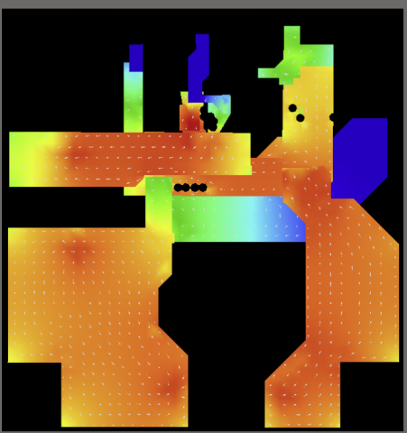
The layout for this design is implemented with the following block diagram in a four‑layer PCB. The block diagram shows the basic approach for locating all of the components in order to separate the RF, digital, and power sections.
In the finalized PCB layout, larger power rail sections are routed on layer 3 and smaller portions are routed on layer 1 to make connections between some of the components. The RF signals and most of the digital signals are routed on layer 1, and a portion of the interface to the NFC chip is routed on layer 4. The completed PCB layout is shown below.

Due to the number of power rails and the fact that one rail might demand somewhat high current, I felt this was a good opportunity to demonstrate appropriate use of a four‑layer PCB stackup with a SIG/GND/PWR/SIG stackup.

For the moment, I would prefer to zoom in on part of the routing on Layer 4. There is a group of digital signals which has been routed on layer 4 in order to connect the microcontroller to the NFC chip. You'll notice that these signals are all routed over a solid section of power rail. Furthermore, these signals are mostly low‑speed signals with only a few signals being part of an SPI interface. The lower‑speed configuration signals and the I2C bus will not cause emissions problems and are unlikely to have a susceptibility problem. The SPI interface runs faster, but the thin outer layer dielectric ensures strong suppression of radiated emissions.

To help provide a reference net for the signals on layer 4, copper pour has been used on this layer as shown in the above images. Running this copper pour alongside the traces on layer 4 ensures that the faster signals have a low‑impedance return path and thus strong suppression of EMI.
Because copper pour has been used on layer 4, it also needs to be used on layer 1 to ensure copper in the stackup is balanced. This will help prevent warpage when the PCB stackup is fabricated and pressed. Finally, stitching vias are placed to connect the internal ground with the top and bottom layer copper pour near the faster high-speed signals, particularly the SPI vias and the oscillator vias.
Antenna Feed Line Clearance
The final point to discuss in this design concerns the clearance to the RF feed line. This clearance is quite important because the copper pour and the RF feed line on the top layer form a coplanar waveguide. The coplanar waveguide requires some clearance to be set to maintain the feed line impedance at 50 Ohms. This clearance and the required trace width can be determined from inside the Layer Stack Manager.
The Layer Stack Manager calculation for the RF feed line impedance is shown below. Here we can see that the trace width must be set to 6.5 mil and the clearance must be set to 6 mil. This will ensure that the antenna feed line is narrow enough to route directly into the U.FL connector for the external NFC antenna module.

Normally, we would need to enforce a trace width design rule and a net‑specific clearance design rule for the RF feed line in the PCB Rules and Constraints Editor. as shown below. However, I have used a spacing value that matches the default spacing for in my PCB layout, so I do not need to create these additional rules as long as the trace width is set to the right value.
Whether you need to build reliable power electronics or advanced digital systems, use Altium’s complete set of PCB design features and world-class CAD tools. Altium provides the world’s premier electronic product development platform, complete with the industry’s best PCB design tools and cross-disciplinary collaboration features for advanced design teams. Contact an expert at Altium today!

About Author
Related Resources
Related Technical Documentation
Table of Contents
Design to Release, Without the Friction
- Keep reviews tied to the right version
- Reduce handoff confusion and rework
- Spot sourcing and release risk earlier
- Work solo, share when needed
Get Started
Thank you, you are now subscribed to updates.

