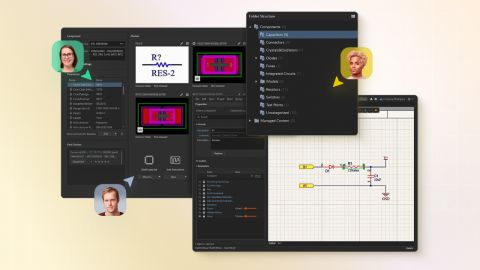


This article explains how to create, find, place, organize, edit, and manage snippets in Altium Designer using the Design Reuse panel. It covers both Workspace and local snippets, shows how snippets can capture schematic or PCB circuitry for reuse, and outlines the key actions available for maintaining them, including folder organization, revision-related details, and management options for…
Parent page: More about Schematics Related Resources Multi-Sheet and Multi-Channel Design Compiling and Verifying the Design Design Synchronization It's the components and how they connect to each other that creates your unique, electronic circuit. In the schematic you create the logical representation of your design by connecting the component pins together, to design the printed circuit board…
This reference page walks through the PCB query keywords in Altium Designer that work with parameters, showing how to find components, footprints, and other PCB objects based on parameter names and values. It covers keywords for checking whether parameters exist, matching specific values, retrieving string values for filtering, and converting parameter text into numbers for comparisons such as…
This reference page walks you through the Membership Checks category of query keywords available in Altium Designer for PCB and PCB Library documents, showing what each keyword does, how to write the syntax correctly, and what kinds of objects each query returns. It covers unit conversion functions such as AsMils and AsMM, along with object and property matching functions like…
This reference page gives you a clear, practical guide to the Layer Checks category of query keywords available in Altium Designer for PCB and PCB library documents. It shows what each keyword returns, how to write its syntax, and how to use true and false conditions to include or exclude objects on specific layers such as top, bottom, paste, silkscreen, solder mask, signal, plane, and mechanical…
This reference page walks you through the Attribute Checks category of query keywords available in Altium Designer for PCB and PCB library documents, showing how each keyword is used to find component objects based on pad rows and columns, centroid positions, and pin counts across different layer types. It is a practical lookup resource for understanding the syntax, example usage, and returned…
This article explains why pin package delay matters in high speed designs, especially above 500 MHz, and shows how Altium Designer lets you account for that delay using Pin Package Length or Propagation Delay values in both the schematic and PCB editors. It walks through where this delay information comes from, how those values affect signal length and routing delay calculations, how they…
This article explains how Altium Designer applies design rules to xSignals, with a focus on high-speed PCB work where length accuracy and signal timing matter. It walks through how Matched Lengths, Length, and Return Path rules can be targeted to xSignals, how to approach tuning when your xSignals include both single nets and differential pairs, and why accurate route length calculation is…
This article walks you through how to manage xSignals in Altium Designer using the PCB panel, including how xSignal classes, individual xSignals, and their primitives are organized and displayed. It highlights what information you can view for each xSignal, how visibility and color can be controlled, how signal and routed lengths are calculated, and how to inspect primitives and delete xSignals…
This article explains what xSignals are in Altium Designer and walks through the practical ways to create them, with a strong focus on the xSignals Multi-Chip Wizard, the most common method. You will see how xSignals can be defined between pads, components, connected nets, and even within existing xSignals, along with how naming, classes, and rule setup are handled in the PCB environment. The…
Learn More