


Navigating the Bend and Fold in Flexible Circuit Design

At a Glance
In this informative article, Tara Dunn looks at the advantages of utilizing flexible circuits in electronic design, with a specific focus on their ability to be bent and folded. Mentioned are essential factors to consider when designing flexible circuits that can withstand folding without compromising functionality and reliability.


In the ever-evolving world of electronics design, flexible circuits continue to gain popularity as a transformative solution. For an overview of the many benefits of flexible circuits and rigid flex constructions, here is a link to a previous blog. Today, we are going narrow in and focus on one of the most obvious benefits: the ability to bend and fold these materials. We will look at mechanical, electrical and materials considerations that shape flexible circuit design and ensure we are not compromising functionality and reliability when introducing bends or folds into the PCB design.
There are several key elements to consider ensuring the circuit can be folded, aligned and assembled correctly without causing stress of damage:
Folding Zones Definition: Identify the areas where the flexible circuit needs to be folded. These should be clearly defined as “folding zones” in the documentation package and marked in the layout to be sure that they are clearly recognized during manufacturing and assembly.
Bend Radius Calculation: Determine the minimum bend radius based on material selection and stack up and confirm this meets industry standard guidelines. The bend radius is the curvature that the circuit can safely tolerate without cracking, delamination or excessive stress that could lead to a failure.

As an example, with a double-sided circuit with an overall thickness of 0.012” the minimum bend radius would be 0.072”.
While flexible materials are designed to be bent, flexed and folded, there is a limit to the stresses the material can withstand and exceeding these limits can result in delamination and conductor fracture. Standard guidelines are:
Single-sided construction: 3-6x’s the circuit thickness
Double-sided construction: 6-10x’s the circuit thickness
Multilayer construction: 10-15x’s the circuit thickness
Dynamic application: 20-40x’s the circuit thickness
Clearance and Tolerance: Design your folding areas with sufficient clearance to accommodate the bending radius without causing stress on traces, vias or components. Provide a buffer zone to prevent strain on these elements during folding.
Component Placement: Avoid placing components too close to folding areas to prevent damage or stress during bending. Keep critical components away from these regions.
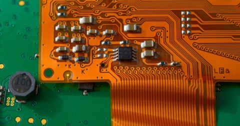
Via Placement: Vias should be placed carefully to avoid critical bending areas. Placing vias in the bending zones can cause stress concentration which can lead to failure.
Trace Routing: Try to route traces perpendicular to the bending direction whenever possible and use wider traces in the bend areas to distribute stress over a larger area. Do not transition layers in the bend area and avoid overlapping traces between the different layers to minimize stress.
Alignment Features: Incorporate alignment features like notches, registration marks or holes into your design to aid in accurate folding and alignment during assembly. These features provide a visual guide for assemblers.
Folded State Simulation: Simulate the folded state of the flexible circuit to ensure that no traces or components will be overstressed.
Folding Test Prototype: Create test prototypes to physically fold and unfold the flexible circuit. This will help verify the design and identify any unforeseen issues with folding, alignment, or component interference.
Stress Concentration Points: Identify potential stress points such as sharp corners or edges in the folding areas and modify the design to minimize these stresses.
Folded Area Reinforcement: Depending on the flex circuit design, consider additional layers of flexible materials or reinforcement in the folded areas to distribute stress and provide mechanical support.
Attachment Methods: Determine how any folded sections will be attached together. There are multiple options: adhesive bonding, heat sealing, and mechanical fasteners as example.
Documentation: Clearly document the folding process, including step by step instructions and visual aids for the assembly team. This should address how to fold the circuit, align the sections and secure them together.
Communicate with your Fabricator: Work closely with your flexible circuit manufacturer to discuss folding requirements and the assembly process. Their expertise and suggestions come from years of experience, and they should be happy to assist.
In flexible circuit design the art of navigating bend and fold areas is a true testament to the need to fuse creativity and precision. The list above captures a list of “best practices” to help balance the mechanical and electrical requirements of a design. It would be fantastic if simply following these guidelines would result in fully functional flexible circuit design on first pass. In “real world” application, there are many things that can impact successfully navigating the stresses on the flexible circuit as it is bent and folded. When things don’t go as planned with the initial prototypes, lean on your PCB fabricator for advice. The more information that can be shared with them, including pictures and videos of the full box assembly will help them suggest solutions. Perhaps materials need to be adjusted, perhaps a button plate process is required for this specific design…..their hard-won experience provides many options in their toolbox.
About Author
Related Resources
Related Technical Documentation
Design to Release, Without the Friction
- Keep reviews tied to the right version
- Reduce handoff confusion and rework
- Spot sourcing and release risk earlier
- Work solo, share when needed
Get Started
Thank you, you are now subscribed to updates.

