Understanding Copper Weight and Thickness in PCB Design

At one time it was a simple process for printed circuit board designers to get their design manufactured. Board sizes and layer stacks were more generic, and usually, someone else made all the hard layer configuration choices for you. It is a completely different game now with multi-layer PCB designs ranging from two to over thirty layers. In addition, trace widths, ground planes, hole sizes, substrate materials, characteristic impedance, dielectric constants, thermal resistance, and even solder mask and solder paste requirements can all have an impact on your circuit board’s stackup. You need to know those factors that will affect your PCB stackup design so that you can make the correct layer decisions upfront for your PCB layout.
To help we’ve included some PCB copper thickness guidelines below that will give you a better understanding of what you need to know in order to create the best possible layer stack for your design. Additionally, we will look at the tools and resources within Altium Designer that will help you to define your PCB design layer stack. Finally, we will look at the manufacturing side and help you to understand how Altium Designer can help you to create the documentation that your manufacturers will need in order to build your design.
What to Know about PCBs and Copper Thickness
There is a lot that goes into the fabrication of a printed circuit board, much more than the standard trace thickness, vias, and pads that we are familiar with as PCB designers. You need an accurate understanding of what is involved in a cross-sectional area of your design in order to specify the PCB materials and thickness that will be used in the construction of the final board. You may have a lot of questions on the process, such as what are standard sizes of PCB traces, how does copper weight impact printed circuit board production, and how thick is heavy copper on a Printed Circuit Board, and what is its relationship to heat and temperature rise? To help with these questions and to learn more about copper foil and copper plating, we have included three documents below to get you started. These will give you a better understanding of what goes into the creation of the PCB design layer stack and open the door to you for more research.
PCB Copper Thickness Guidelines
Don’t leave your PCB thickness down to short-term memory and information available on components. To create the perfect layer stack for your PCB design, you need as much information on PCB copper thickness guidelines as possible.
- Start right with these basic guidelines on what goes into a PCB design layer stack.
Learn More about getting the layer stack of your design right.
- High-speed designs need more care in creating their layer stacks. Here are some details on what goes into them.
Learn More about engineering the layer stack of a high-speed design.
- The layer stack needs to be configured to give you the best copper pads and copper traces possible. Here’s more information on how to avoid coper layer defects.
Learn More about potential problems with copper layer defects in your PCB design.

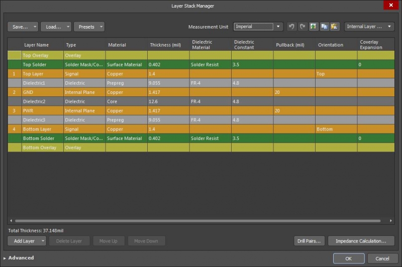
The Layer Stack Manager in Altium Designer will help you to set up your PCB layers accurately
Altium Designer Will Help Determine PCB Copper Thickness Questions
Once you’ve determined what the fabrication process will be for your PCB design and what configuration your board layer stack will be, you will need to assign those layers in your design system. Altium Designer gives you tools to help you determine what your layer stack should be, as well as a layer stack manager to assign materials to the layers and specify copper thickness on your Printed Circuit Board. Once you’ve set it up, you will also find that Altium Designer gives you the best functionality for interactively routing traces on your PCB layers. Altium Designer has been created to help PCB designers like you to set up and accurately design printed circuit boards for the most error-free manufacturing possible.
PCB Copper Thickness Design
Whether it’s traces and trace width, pad size, or hole-size and cross-sectional area, you’ll want layout software that can make your circuit board get printed easily. Altium Designer gives you the ability to set up your design with the specific layer stack and copper weight specifications for fabrication.
- See how Altium Designer can help with the creation of a layer stack for your design with these tips on how to set up the layers in a rigid-flex design.
Learn More about creating a layer stack for a rigid-flex design in Altium Designer.
- Altium Designer comes with many helpful features such as high-speed design setups which will help you work with the layer stack manager in creating a layer stack.
- Once your design is set up the way you want it, Altium Designer’s intelligent interactive routing tools will get your trace routing done precisely to the mils or millimeters that you have specified.
Learn More about routing traces on different design layers using Altium Designer.

Altium Designer’s Draftsman will free up your time by auto-generating precision manufacturing drawings
Communicating Copper Weight and other Data to Your PCB Manufacturers
Setting up your design for precision is one part of the battle, and completing the design to your specifications is another part. There is still one more hurdle to overcome though, and that is in sending the correct and accurate Gerber files, drawings, and other design documents to your manufacturer. Once again, Altium Designer shines here with its ability to create and package the manufacturing documentation that you need in order to get your boards built as you want. Altium Designer gives you the functionality to panelize your designs, auto-generate manufacturing drawings, specify different design variants, and package them all up automatically in reusable configurable batch job output files.
Altium Designer Has the Tools You Need to Send Printed Circuit Board Designs to Your Fabricators
Ensure each pad is placed properly on whatever plane they are being placed on. Whether you’re working in units of mil or larger, Altium Designer has any feature you need to get your design produced.
- After spending time to perfect your design, the last thing you want is a bad board due to something simple such as an incorrect surface finish or bad solder joints. Here is some information on how to avoid manufacturing errors by communicating the right information to your vendors.
Learn More about what kind of information you should be sending your manufacturers.
- Why spend time creating manufacturing drawings from scratch for each design? Altium Designer’s Draftsman was created so that you can automate this process and focus more time on the actual design.
- Instead of recreating the same design over and over again, Altium Designer’s variants feature will allow you to create design variations from the same database.
A lot needs to go into your PCB design in order to get it manufactured with as few errors as possible. Altium Designer has the tools and functionality built into it to help you achieve this goal.


