


The Beginner's Guide to PCB Power Integrity: From Board to Package

At a Glance
In this article, we give a complete overview of power integrity, starting from the PCB and including everything up to packaging.


As pedestrian as it may seem, power delivery on the PCB and in advanced packages remains one of the biggest challenges facing designers, particularly in environments like data center, edge computing, mobile devices, and telecom/networking. Massive amounts of data are being moved through extremely high data rate channels in these environments, and as much as we focus on signal integrity, none of these systems will work without stable power.
Power integrity occurs at the component level and at the PCB level, and as others have mentioned in this blog, power integrity problems can create signal integrity problems (jitter, supply/ground bounce, EMI). While most of the simpler power integrity guides tend to focus only on the PCB level, both the PCB and the package must work together to provide stable power to interconnects.
This guide will attempt to give a comprehensive conceptual view of power integrity for PCB designers. While designers generally don’t have control over their packaging, they can take steps to ensure their PCB and component packages work together to provide stable power. I’ll outline some of the main approaches to ensuring power integrity across these domains, spanning from stackup design to optimal capacitor selection.
What Determines Power Integrity in a PCB?
Power integrity is a concept in both AC and DC; in the DC case, we care about whether copper rails are properly sized to ensure low DC voltage drop. When a PCB is not designed with power integrity in mind, the voltage observed on a power rail could look like the image shown below. During the phase where I/Os are switching, the current pulses being pulled from a PCB's power delivery network (PDN) excite transients on the power bus. An example under repeated switching of logic circuits is shown below.
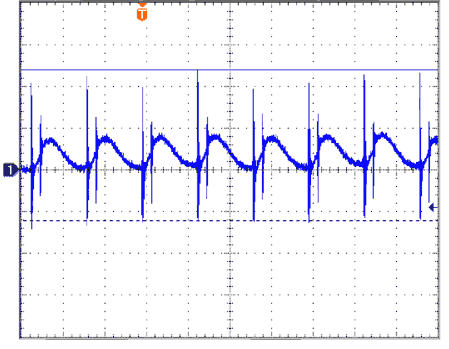
The most common instance where this occurs is in high-speed components that switch very quickly; more I/Os switching simultaneously leads to greater power demands, and thus there can be more noise on the power rails. When you zoom in on one of these transient responses, the transient decays with multiple time constants, most principally a long, low-frequency time constant that contributes the most noise on a power rail.
In general, when the signal rise time is faster for a given PDN structure, the ripple that is generated could have greater overshoot, or multiple time constants associated with higher frequency underdamped oscillations. These oscillations are undesirable for two reasons:
- They appear as noise on output signals (both timing noise and signal level noise) that could cause logic levels to be misinterpreted
- They create radiated EMI that can be measured from the board, typically from the edge
For both reasons, designers must take some steps to ensure the DC voltage output from regulators will be as stable as possible.
PDN Impedance, Inductance, and Capacitance
The impedance of the PDN in a PCB will be the major determinant of power integrity. Regulators also play a role through their feedback loops (see below), but designing the PDN impedance is the domain of the PCB designer. The goal is to have as low a PDN impedance as can be feasibly reached, typically below 100 mOhm levels.
PDN impedance is determined by the presence of several elements, as summarized in the table below.
|
|
|
|
|
|
|
|
|
|
|
|
|
|
|
|
|
|
Collectively, these elements will determine the impedance spectrum of a PDN. The various contributors to a PDN are shown in the image below, and these contributions are delineated roughly by frequency range. This impedance spectrum shown here is constructed from a large number of capacitors, which is typical of digital processors with high I/O count running at fast edge rates.

PDN Topology
All PDNs supplying power to advanced processors are multiport networks. They require multiple regulated voltages, spanning from high values to low logic levels. It is common to see voltages spanning from higher logic levels (5V0 or 3V3) down to as low as 0V8 on high pin count processors.
An example power tree defining the PDN of an advanced processor is shown below. The example intends to show how different rails can be constructed coming from a main power supply or regulator supplying power to the entire system.

The above example is not intended to be generalized to all digital components, but it should illustrate the point that many components will have multiple rails. A digital processor being supplied by the above power topology could be any type of component, such as a large FPGA, network processor, MPU, large MCU, GPU, or another specialty processor. The I/Os on the processor are pulling their power from the supply rails, so it is these rails that can experience significant transient noise in the PDN.
The above topology should illustrate the need for two design requirements: isolation between rails, particularly two different rails supplied by the same regulator, so that they do not transfer noise between each other. Each rail also needs to have its own low impedance value to ensure any excitation of noise is low.
PCB Stackup and Materials
In terms of power integrity, material selection in the PCB stackup plays an important role in providing the capacitance required to ensure stable power delivery. In addition, the layer arrangement should provide power rails to be placed adjacent to ground planes on thin layers. This will help ensure the stackup provides sufficient capacitance for signals up to approximately 1 GHz signal bandwidths.

When there is insufficient capacitance available in a plane layer, and when discrete capacitors are limited by parasitics, the required capacitance can be provided by an embedded capacitance material (ECM). These materials are very thin films (some below 1 mil thickness) with high Dk values reaching up to 30. These materials can also have very high losses that will absorb EMI propagating in the PCB substrate, thus reducing radiated EMI from the board edge.
In terms of the PDN impedance, the effects of these materials is four-fold:
- Provide higher capacitance and thus lower impedance in mid-range frequencies (up to 1 GHz)
- Move PDN resonances associated with the power/ground plane pairs to lower frequencies
- Dampen PDN resonant peaks in the GHz range associated with power/ground plane pairs
- Move the PDN impedance valley (from 0.1 to 1 GHz) associated to the plane capacitance to lower frequencies
The effects of these materials can be seen in the graph below. As the dielectric thickness decreases, we can see that the resonant peaks in the PDN dampen and move to lower frequencies. Similar results can be seen if we increase the dielectric loss in the material.

Package Parasitics
Component packages have their own parasitics related to the structure of the package, and component packages have their own PDN impedance. The impedance of the package combines with the impedance of the PCB, and together these will determine the amount of noise seen at the supply input in logic circuits on the semiconductor die. Modern processors include in-package capacitors to help dampen transient excitations and extend useful signal bandwidths deep into the GHz range.
Beyond the PCB and Packaging
We’ve covered everything across the PCB and packages, including some of the most intricate design features and models in advanced packaging. The PCB designer has control over the board layout, stackup, and placement/routing, and they have some control over the package. In terms of power regulation strategies, we have not covered two important topics:
- Voltage regulator modules (VRMs) for large high-speed processors
- Simulations in the schematic and PCB layout
VRM Modules
The structure of a PDN and the fact that many advanced components require multiple power rails requires multiple regulator modules, which branch in parallel with each other. The job of a fixed power regulator is to compensate voltage droop and maintain a target output voltage through a feedback loop (FB pin on most regulators). The feedback loop must respond quick enough and modulate the output in an attempt to stabilize the output voltage.
The factors contributing to regulator feedback loop response appear at the layout level and component level. I’ve discussed some of these points with Steve Sandler in a recent episode of the OnTrack Podcast.
The topic of VRMs and their layout practices will be presented elsewhere on this website. Aside from VRM design and layout, designers should focus on designing the right stackup and capacitor/material selection to ensure low enough PDN impedance within their operating bandwidth. As we discussed above, layout and placement will also affect power integrity through creation of parasitics.
Simulation
Simulations can be performed in AC or DC, and in the schematics or the finished PCB layout. For high-speed PCBs operating with up to GHz signal bandwidths, AC power integrity simulations are most important as they can reveal power bus ripple when I/Os begin switching.
AC simulations in the schematic are SPICE-based simulations examining stability of the capacitor network used for decoupling/bypassing. These models allow for an estimation of the power bus response, as well as an evaluation as to whether the capacitance included in the PDN will be sufficient. There is also the matter of evaluating isolation between different power rails fed by the same regulator/VRM, which can be determined by evaluating the transfer impedance.
To learn more about PDN simulations in schematics, including the use of ferrites, watch the playlist below.
AC simulations can also be performed in the PCB layout, but this requires an electromagnetic field solver to predict signal behavior in space and time given the structure of the PDN in a PCB. These simulations are computationally intensive and they require specialized software.
Although AC simulations are important in advanced products, DC simulations still matter in high-speed PCBs. The high number of I/Os that switch in the main processor in these PCBs can create multiple Amperes of current demand. When you get to a very large high-speed board serving multiple peripherals, like a backplane, you now have to support on the order of ~100 A of current throughout the system, including on power rails supplying I/Os on fast processors. Therefore, it’s important to identify and eliminate extreme currents in power rails.
The CAD tools in Altium give every user and engineer the ability to take control of their power integrity and delivery strategy. Altium is the industry’s leading CAD platform that also provides integration with cutting-edge applications for SI, PI, and EMI/EMC simulations. When you’ve finished your design, and you want to release files to your manufacturer, Altium makes it easy to collaborate and share your projects.

About Author
Related Resources
Related Technical Documentation
Table of Contents
Design to Release, Without the Friction
- Keep reviews tied to the right version
- Reduce handoff confusion and rework
- Spot sourcing and release risk earlier
- Work solo, share when needed
Get Started
Thank you, you are now subscribed to updates.

