Minimize Propagation Delay in Logic Gates: Synchronize Pulse Trains
When you have an analog watch, daylight savings time can wreak havoc in your personal and professional life. You might wake up and not even realize that you are an hour off schedule. No one wants to admit that they have fallen victim to daylight savings time, and your entire schedule has to resynchronize when this happens.
Synchronizing your clock and your electronics components is critical in high-speed PCB design. Applications like bus trace routing, high-performance DDR memory, and any high-speed circuit, in general, require precise timing of signal and clock pulses. Propagation delay in logic gates, such as a xor gate or NAND gate, can corrupt data and place critical components out of sync with the system clock. Additionally, setup and hold times require precise routing of clock and signal traces. If any of the supply voltage gets held up with a gate delay or the like, any integrated circuit can experience issues. But what is propagation delay in digital electronics?
Setup and Hold Times
Propagation delay in logic gates typically refers to the rise time or fall time in logic gates. This is the time it takes for a logic gate to change its output state based on a change in the input state. It occurs due to inherent capacitance in the logic gate. In the past, when clock and data transmission rates were slower, propagation delay typically did not cause major issues in digital circuits because the rise and fall times were comparatively faster.
Nowadays, the situation is not as convenient. High-speed circuits can have clock frequencies that are comparable to the propagation delay in digital electronics. The result is that data moving around the system may be out of sync with the clock, such as from a logic gate propagation delay, which can wreak havoc on your device. Components may not operate as designed due to this mismatch. Logic gate propagation delay, or any other type of propagation delay throughout any circuit, can also cause data corruption in data-intensive applications.
As an example, consider a rising edge flip-flop that is configured to toggle on the next clock pulse. When the rising edge of the clock pulse arrives, the output state will begin to toggle. But the output state does not immediately switch. Instead, the output state takes some time to rise from 0 to 1, or vice versa. This means that the output pulse and the clock pulse downstream from the flip-flop are likely to be out of sync.
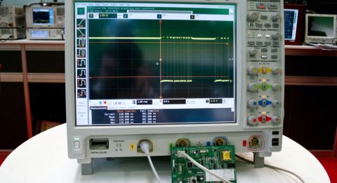
Propagation delay can be measured with an oscilloscope
Compensating for Propagation Delay
Obviously, you can’t speed up a clock signal in a digital system, nor can you selectively speed up clock pulses in different of your PCB. But you can delay the arrival of different signals in your device by adjusting trace lengths. Adding a small extension can delay a pulse just enough to bring your signals back into sync. Delaying the clock trace just slightly will give your ICs time to settle into the proper state and still remain in sync.
Proper compensation also requires calculating the clock skew between different components in your PCB. Most likely, your PCB runs off of a global clock that feeds directly to different components. Depending on how traces branch off to different components, clock skew can accumulate, requiring greater setup and hold times to synchronize clock and signal pulses.
One method that can give your signals enough time to reach full level before the next clock pulse is to meander your clock trace at certain points in your PCB. A serpentine meander can give your clock pulse just the right delay. Differential traces must have meandered together and close coupling must be maintained.
Give your devices the traces they need to thrive
So how do you choose which traces to meander? Compensation should be applied to traces in each net. First, look for the longest signal trace length within a net, and meander the remaining traces so that the signals are synchronized across all traces. Finally, adjust the length of the clock trace that connects to the components in this net. Delay the clock pulse by just enough time so that the ICs can rise up to full voltage.
Line Delay and Rise/Fall Times
Line delay and propagation delay in digital electronics are sometimes used interchangeably. Line delay has an important relationship to propagation delay and can create signal transmission problems under certain conditions. Specifically, the rise or fall time of the output signal should be compared to the line delay over the output trace. When the trace length is long, the output signal moves as a traveling pulse and can be reflected at an impedance mismatch.
Signal traces must be treated as transmission lines under certain conditions. One industry rule of thumb is to terminate the output signal trace from a logic IC when the one-way line delay of the PCB trace is equal to or greater than half of the signal rise/fall time (whichever edge is faster).
This means you can get away with an impedance mismatch as long as the circuit signal trace is short enough. When the trace is short, the signal rises up to its full voltage level and the output voltage is applied across the entire trace. Rather than a traveling pulse, the signal exists as a momentary constant voltage between two points and there is no signal reflection.
A great piece of PCB layout software like Altium Designer® makes it easy to lay out your next basic circuit or complex high-speed design. The integrated component libraries and the ActiveRoute® tool can help you avoid problems from propagation delay in logic gates.
If you are interested in learning about how Altium Designer can help you build your next high-speed device, talk to an Altium Designer expert today.


