


Rigid-Flex PCBs in IoT Devices: ECAD and MCAD Collaboration


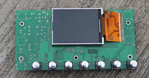
At a recent PCB manufacturer’s trade show, multiple fabricators informed me they are seeing many more requests for flex and rigid-flex PCBs recently, particularly for smart wearables and small embedded/IoT products. The advantages of flex and rigid-flex PCBs include more efficient use of space in an enclosure, and the ability to adapt to foldable devices. Whether you need a static or dynamic flex/rigid-flex PCB, you’ll need to verify a number of aspects of your board within your design tools before manufacturing.
Design verification requires more than just looking at conformance to electrical design rules. Sure, electrical functionality is important, but rigid-flex boards that will fit into foldable products, or any other movable enclosure, require multiple levels of mechanical design and verification to ensure they will meet product design requirements. Here’s what you should watch for in your rigid-flex design during mechanical verification and how integrated MCAD tools help you build better products.
Clearances in Rigid-Flex PCBs
These two aspects are critical when you’re trying to save space in an enclosure and prevent portions of your enclosure or board from colliding. Your typical ECAD tool only gives you a 2D view of your CAD layout, providing only a view of traces, pads, and component outlines. You’ll obviously need this for your layout, but you’ll be unable to see how your components fit together in the vertical direction. It’s important to spot whether various components will collide when assembled, and whether mechanical components will fit into your board and in your enclosure.
Consider the case of DPAK components, large heatsinks that span beyond the edge of a component, and connectors with locking side tabs. Some design software will allow you to place bulky capacitors or other components that stick up above the board very close to large mechanical components. Although this does not technically violate any electrical design rules, it creates a risk that these components would collide during assembly. Unless you have access to an MCAD tool in your PCB design software, you’ll have to rely on your manufacturer spotting this overlap before beginning manufacture.
There is another aspect to consider in high voltage designs, which relates to clearances between components in 3D. IPC-standardized creepage and clearance distances are calculated along the surface of the board and between components above the board. Depending on the size and span of mechanical components, specifically in the vertical direction, it may be difficult to calculate the clearance and creepage distance by hand. You’ll have to resort to an assembly drawing, or you’ll need to import your board and STEP models into an external mechanical design application.
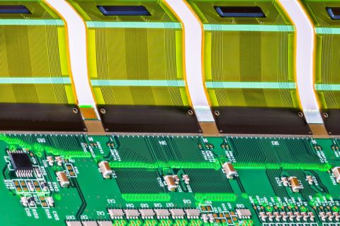
This all becomes compounded in rigid-flex PCBs, as colliding components will prevent a flex ribbon from reaching the desired bend angle or radius. If you can spot clearances between components on the board, and between rigid-flex or flex sections of the board, you can prevent a fabrication delay. It’s best to spot these points early during the design phase. With the right design tools, you can actually construct your layout in 3D, allowing you to accommodate bulky components and ensure clearance early.
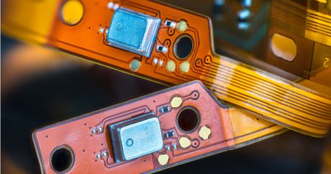
CCD array on a flex PCB
Fit to Enclosure and Structural Integrity
With dynamic flex and rigid-flex PCBs, conductors on the flex sections need to be properly designed to prevent permanent deformation and fracture as the ribbon is flexed. As the ribbon is flexed, the components need to have sufficient clearance in order for the board to move through the full range of motion. Similarly, with static deformation, you need to design the board so that the aforementioned clearances are satisfied. This is particularly important in high voltage rigid-flex PCBs, which must comply with creepage and clearance standards. Although these devices are somewhat rare, you still need to watch for clearance requirements between different sections of the board if they are folded together.
When you have access to a set of mechanical design tools that integrate with your electrical design and layout features, you can examine the fit and function of your rigid-flex board alongside the mechanical enclosure. Using something like Solidworks allows you to import a 3D model of your board and examine it alongside your enclosure design. The bending lines and flex sections you define in your ECAD can then be animated and examined for clearances in your MCAD application. This lets you spot which components, if any, need to be swapped out in order to ensure the board fits to the enclosure and your device functions as desired.
New products are becoming progressively more advanced, and mechanical and electrical design teams need to work together, especially when designing products with rigid-flex boards. These multifunctional teams also need access to data management and collaboration tools that allow easy sharing of component and design data, as well as seamless sharing of design updates between team members. Once you add a set of tools that provides component sourcing data into the mix, design teams have a complete set of features they need to manage all aspects of a new design and remain competitive.
Designing rigid-flex PCBs and performing important verification steps is much easier when your PCB design software includes top-notch MCAD/ECAD collaboration tools. The world-class PCB design tools in Altium Designer now integrate with the data management and MCAD collaboration features in Altium Concord Pro™, giving you a complete PCB design and management solution in a single program. You’ll also have a platform that synchronizes ECAD/MCAD co-design for any application, including rigid-flex PCBs.
Contact us or download a free trial of Altium Designer® and Altium Concord Pro. You’ll have access to the industry’s best layout, MCAD collaboration, and data management tools in a single platform. Talk to an Altium expert today to learn more.

About Author
Related Resources
Related Technical Documentation
Table of Contents
Design to Release, Without the Friction
- Keep reviews tied to the right version
- Reduce handoff confusion and rework
- Spot sourcing and release risk earlier
- Work solo, share when needed
Get Started
Thank you, you are now subscribed to updates.