SpaceX and Other Advanced Technologies Require Multi Board PCB and CAD Software Innovations
When I was in middle school I used to love to build and fly model rockets. We had a rocket club at school and except for the number of rockets that I littered the trees with, it was a lot of fun. One thing was certain though, although the rockets we launched went up, no one knew exactly where they might come down. Suspended by their parachutes (assuming that those chutes actually deployed as intended), they might land anywhere.
Recently I watched as the two side boosters of the Falcon Heavy from SpaceX executed perfect simultaneous landings under their own power. These boosters were not dangling under parachutes with the hope of hitting near to their landing zones, they used their remaining fuel to soft-land exactly where they were programmed to. The lesson that I learned as a middle schooler, that rockets go up but who knows where they’ll come down, had been redefined.
For years I’ve been designing printed circuit boards, and I’ve always designed them one board at a time. It was the only way to do it, as multi-board system level design was beyond what our CAD systems could do. Today though, that fact has also been redefined.
As technology evolves, our design methodology needs to change along with it so that we are ready for it. We now have the ability to design multiple boards within a project to give us system-level design. This will give you significant advantages over single board design. System-level design like this is going to be essential as we design the latest advancements in technology exemplified by the Falcon Heavy and other aerospace applications.
More Than Meets the Board: Multi-Board PCB Innovations
The standard for PCB design has always been to design one printed circuit board at a time. These designs were often part of multi-board systems, but due to the limitations of our PCB CAD tools we only had visibility into the design that we were currently working on. Although we knew that there were other designs involved, we couldn’t see them and had to rely on input from other sources to match our work up with the rest of the system.
The mechanical engineers would give us board outlines with keep-out zones so that we could avoid potential placement conflicts. This would tell us where not to place components over a certain height, or in some cases not to place any components at all. In the same way, the electrical engineer would match up net names from different designs and the schematics would indicate which connectors would pair up between designs.
The Challenges of Designing Multiple Boards for a System
The input from mechanical and electrical engineers went a long way towards helping us to design a single PCB so that it worked together with the rest of the system boards. The drawback, of course, was that those directions were still a little vague. It was sort of like driving down the road and seeing a “caution” sign. What are you supposed to be cautious about? We needed more details in order to do a complete job in design.
Take placing connectors for instance. It is easy to place a connector at a specified location, but without the ability to look at it in relation to what it is connecting too you may miss some important design details that could be cleaned up. Is the connector in the best location? Will the connector harness reach the way it is supposed to? With the harness plugged into the connector will that cause any unforeseen difficulties with the surrounding placement?
Another area of design that was a challenge was in designing the circuitry. It is a regular function of PCB design to create good inter-board connectivity with placement and routing. It is more difficult though to design for intra-board connectivity without the ability to work with multiple designs simultaneously. What may seem like a great placement and routing scheme on an individual board may change a little when looked at from a multi-board system perspective.
How Design Tools with Multi-Board PCB Innovations Can Help
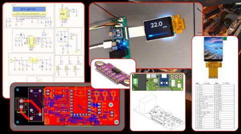
Fortunately, there are PCB design tools today that allow you to design from a system level perspective. By starting at the project level, you can designate the individual PCB designs below that for all of your system boards. This gives you the ability to specify net names that will cross between the designs so that you can work with consistent net name connectivity between designs.
On the layout side, you can either work on designs individually, or you can work at the project level bringing them all together as they would appear in the final system. This gives you the ability to adjust your component placement according to the needs of the actual system instead of relying only on “keep-out” zones.
Multi-Board PCB design systems like this can make the difference between designing in the blind for a system and actually designing at the system level. With the ability to design within a NATIVE 3D™ environment in the Multi-Board PCB design system, you can see where placement conflicts are and make real-time corrections in order to resolve the problem.
For both the ability to design at the system level and to work in those designs within a 3D environment, PCB design software such as Altium Designer® can be pivotal to your design success. You will be able to see how all of the system boards in your project will work together allowing you to make design changes as needed to resolve layout conflicts.
Would you like to find out more about how Altium can help you with your next system-level design? Talk to an expert at Altium.


