How to Solve Fit, Form, and Function Challenges in Robotics with ECAD-MCAD Collaboration

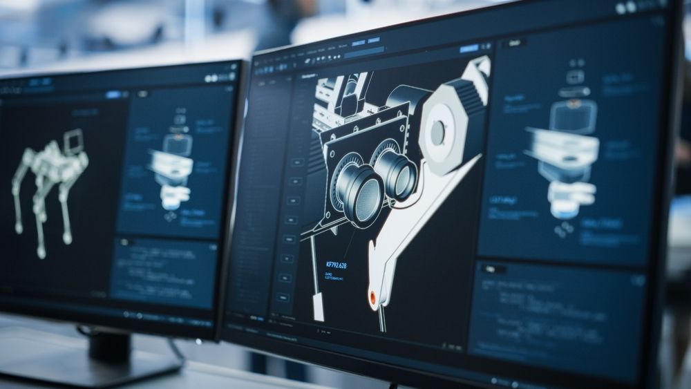
As robotics systems become increasingly compact, complex, and demand higher performance, the traditional boundaries between mechanical and electrical must be broken. Engineers face mounting pressure to ensure that every component, from printed circuit boards (PCBs) and connectors to enclosures and actuators, fits into more complex casing.
Design flaws related to fit, form and function can derail development, increase costs, and compromise product reliability. As robotics designs push the limits of geometry, motion, and enclosure constraints, even the smallest oversights can lead to major setbacks.
Fit, Form, and Function Challenges in Robotics
Fit: In robotics, space is always at a premium. PCBs, flex cables, connectors, sensors, and actuators must be precisely positioned to navigate tight internal volumes, often within curved or mobile enclosures. Overlooking the height or position of components leads to clearance issues, blocked motion paths, or mechanical interferences with moving parts.
Form: The internal and external geometry of robotics systems is often highly customized, varying more and more as teams work to deliver high-functioning electronics for unique applications, including humanoid structures or streamlined drones. Components must match the form factor precisely, and this requires a greater understanding of specifications.
Function: Even with the perfect component fitment, reliability is crucial in real-world applications. Functional failures in robotics may involve signal noise from poor trace routing, thermal buildup in sealed enclosures, or vibration damage to sensitive components. Robotics in industrial, aerospace, and medical environments cannot afford failures or allow incredibly low tolerance.
These three design elements do not exist in isolation. Modifications in one area directly impact another; mechanical packaging can affect PCB layout, thermal behavior, or system performance. This is why ECAD-MCAD synthesis has become essential for anticipating and resolving these challenges before they lead to costly rework or field failures.

Real-World Examples of Fit, Form, and Function Issues
As mechanical engineering meets even more complex needs, new challenges arise as high-power and data-intensive robotics become more compact, and come in uniquely designed packages. These examples highlight the nuances that designers must navigate, which inspires even greater demand for ECAD-MCAD collaboration.
- Connector Misalignment - A surgical robotic arm with a rotating joint must route cables through slip rings or rotating joints. A seemingly minor PCB outline change can shift connector placement, causing misalignment with mating harnesses and impeding rotation or sterilization integrity.
- Enclosure Curvature and Custom Shapes in Service Robots - In many modern instances, flat PCBs must fit inside curved shells or curved mounting surfaces. Without ECAD-MCAD coordination, designers may not catch clearance clashes between component heights and outer casing curvature until later in the design process.
- Thermal Failure in Compact Actuator Controllers - In an industrial actuator, the driver PCB may reside in a sealed metal housing. Mechanical engineers might overlook internal heat buildup; without heat sinks or vents, temperatures escalate, leading to driver failure. Mechanical packaging must consider ECAD-simulated thermal loads.
Where Traditional Robotics Design Workflows Break Down
There are a few areas in which traditional workflows are failing designers, and the wider electronics supply chain. It is important to remember that efficiency in this process sets a precedent for success in all other go-to-market areas.
With discrepancies or delays in the physical prototyping phase comes cost implications and rippling effects that impact lead times. One of the ways in which designers can save time and money is by solidifying their designs prior to the physical prototyping phase, which is better supported by digital twin capabilities, marrying electric and mechanical designs in a digital environment first.
Recurring issues inspiring ECAD-MCAD:
- Design Errors: Both electrical and mechanical designers continue to experience the same issues, which are often the result of poor management in early-stage design.
- Siloed Workflows: Mechanical engineers have historically developed their product form factors with minimal insight into the electrical implications, and vice versa. Oversight from either side results in an overstretched design process.
- Manual File Transfers: Hand-in-hand with the issue of siloed work is inefficient, manual file transfers. This sustained practice eliminates the potential for greater efficiency (i.e. both teams have to work extra hours to address potentially outdated design adjustments).
- Slow Iteration Cycles: As mentioned above, iteration cycles are dragged out by miscommunication between both teams. Rework processes are highly inefficient when compared to that enabled by collaborative ECAD-MCAD solutions.

ECAD-MCAD Collaboration Solves Fit, Form, and Function Cases
The solution to fit, form and function dilemmas can be one of a few capabilities. Modern platforms offer tighter integrated workflows, not to mention improved leverage of digital services, such as:
- Bi-Directional, Real-Time Synchronization: Designers can edit mechanical outlines or enclosure parts, and the PCB outline, mounting holes, or connectors update instantly in ECAD. Similarly, adjustments in the PCB (like movement of components or mounting points) are reflected in mechanical models.
- Shared 3D PCB and Component Models: Components can carry accurate mechanical models and material properties into the MCAD environment. This facilitates clash detection, clearance checking, and alignment with curved geometry or curved mounting planes used in robotic shells.
- Embedded Thermal and Integrity Simulation: Fusion 360 enables e-Cooling analysis, thermal simulation of PCB copper, stackup, and components to detect hotspots before mechanical design completion, critical for actuator or motor driver modules in sealed housings.
- Centralized, Cloud-Based Collaboration: Both teams work concurrently on a single project platform, reducing miscommunication and version confusion. Changes are managed automatically.
Introduction of collaborative platforms has been a game changer. Real-time synchronization between ECAD and MCAD environments cuts development times by eliminating the need to export and reimport data. Leveraging a unified platform that understands and translates both design languages, common errors are minimized, engineers are better aligned, and it can speed up iterations by up to 90%.

How to Prepare for Seamless ECAD-MCAD Integration
There are steps to take prior to onboarding a solution for ECAD-MCAD integration. Aside from the initial adoption, there are some checklist items to consider before doing so.
- Standardize component libraries to ensure that parts data is readable across both design teams. Parts geometry and footprint info must be available from the very beginning.
- Automating version control requires a system that serves both parties.
- Real-time linking of workflows enables mechanical and electrical engineers to work in parallel, catching design issues early on.
- Combining workspaces supports thermal, mechanical stress, and enclosure analysis all before physical prototyping.
The Future Design Protocol for Robotics
The next generation of robust, reliable robotics demands a new, co-development approach. Designers must look to break their silos and build collaborative procedures into their daily work.
Mechanical engineers and their preferred tools are now being integrated directly into the PCB design environment for both teams to accurately cross-reference their work. Real-time synchronization, shared 3D models, and cloud-based platforms are all on the cards for companies that wish to offer smarter, faster, more resilient electronics.
Robotics companies are looking to innovate without compromise on either design element, and designers must respond with the same holistic approach. Those who can bridge the divide between design disciplines will find themselves ahead of the curve before the first prototype ever hits the bench.
Whether you need to build reliable power electronics or advanced digital systems, Altium Develop unites every discipline into one collaborative force. Free from silos. Free from limits. It’s where engineers, designers, and innovators work as one to co-create without constraints. Experience Altium Develop today!


