


Annular Rings for PCB and Nonfunctional Pads: Should You Use ‘em or Lose ‘em?

At a Glance
Annular rings placed as non-functional pads in a PCB can affect via strength and signal integrity. Learn when to remove or keep them in this article.


Annular rings in a PCB form a joint between a trace and the via its connects to. The size of an annular ring is determined by the pad size and the drilling tolerances; the ring of copper that surrounds a via hole after the hole is drilled and plated is the annular ring. All pads attached to a via on a multilayer PCB will have some copper that forms an annular ring unless there is significant wander during drilling, in which case the leftover copper might make an incomplete connection to the hole wall (known as breakout).
When you look at the IPC-2221 standards, or the related IPC 601x set of standards on different types of PCBs, you will see a graphic that shows an annular ring attached to a plated hole wall alongside a stated tolerance. When the annular ring on an internal layer is disconnected from the hole wall, we call it a non-functional pad (NFP). This brings up a natural question: do we need to include non-functional pads, or can we remove these without affecting the reliability of the PCB? This is a question we received on a video, and it deserves discussing in more depth as there is a lot of debate as to the use of non-functional pads.
Annular Rings in Functional and Nonfunctional Pads
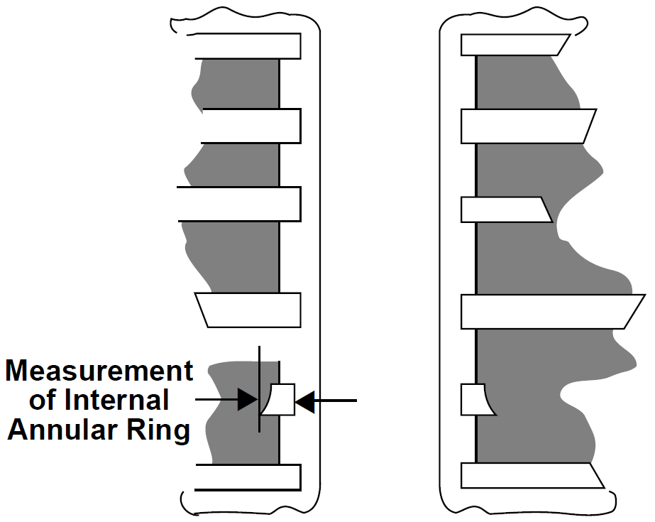
Where does the question of removing non-functional pads come from? If we look in IPC standards on annular rings, the standard seems to suggest that annular rings on internal pads are required to be kept in order to meet the requirements in IPC product classes 1-3. For example, if you look in IPC-6012, you'll see a drawing showing annular rings on an internal layer (See below for the drawing in Figure 3-10 in IPC-6012B). Even though this drawing is only a 2D cross section, it seems to suggest that we are not connecting any traces, which would might infer based on the size of the small pads compared to other pads in the padstack.
Although I have not read the entirety of IPC-2221 or other standards dealing with NFPs, I've never seen a clause stating that they must be included for any IPC product class or under any other standards. That being said, if there are annular ring size requirements that would apply to all lands (functional and non-functional), such as the IPC-6012 Class 3 requirements for high-reliability products. However, there are military aerospace standards that state non-functional pads must be included on all layers as long as clearances abound, so there is a clear question of reliability surrounding non-functional pads. Most of the questions around non-functional pads center specifically around reliability during operation, but manufacturability is another issue; we'll discuss both aspects below.
Why You Would Keep Non-functional Pads
The main justification for keeping non-functional pads concerns their usage as an anchor against each layer in the PCB stackup. The idea is, when the board expands or vibrates, the non-functional pads spread out the stress along the via barrel, rather than allowing stress to concentrate near the center of the via barrel. In high aspect ratio vias that are not formed with sufficient pulsed plating, the center of the barrel can be thinner than the surface regions, so they experience more stress and might crack due to thermally-induced cycling fatigue. However, this is one point that is debated, as was pointed our by an expert panel on CircuitNet.
In summary, there are two main reasons to keep non-functional pads:
- Thermal cycling stability in vias as mentioned above, but this should be tested first
- Thermal stability in solder pads for through-hole components
- It is claimed that non-functional pads thieve current during plating processes, so these would affect thickness of via wall plating
- It is claimed that non-functional pads help plating adhere to the hole
Personally, I would be skeptical about the 3rd and 4th points. Think about all of the designs that have been manufactured on 2-layer boards, or on 4-layer boards with 2 internal planes, which basically have zero non-functional pads on internal layers for signal vias. Whenever someone refers to failure in these boards, delamination from a via hole wall is probably the last thing you would hear. This point probably needs a large asterisk as this might be more noticable when there is repeated thermal cycling, thus we would also expect this to depend on the via aspect ratio.
Why You Would Remove Non-functional Pads
The two points above do not lend a lot of support for non-functional pads, and as I'll discuss momentarily, there are many more reasons to remove them in some boards.
- Known to cause additional return loss and insertion loss increase at high frequencies (multi GHz)
- Possible return loss increase at high frequencies (multi GHz) due to periodic discontinuities
- Takes up space on inner layers that could be used for routing
- Non-functional pads have to be drilled during fabrication, which reduces the life of the drill bit
- Non-functional pads create a problem called "telegraphing" where resin content can be low around the non-functional pads, which will reduce via wall adherence to the substrate
Point #5 appears to go against one of the points in favor of including non-functional pads. This would have to be examined in a microsection test to ensure sufficient resin flow into the region between pads along the via wall.
Do Your Own Testing
Clearly, there is still disagreement as to whether non-functional pads should be included. If they are included, the annular ring requirements should apply; the same requirements apply to functional pads that make a connection to a trace. If you decide to do this as a measure of reliability, then you should compare boards with and without non-functional pads to assess whether reliability is really impacted. The IPC standards (IPC-A-600, IPC-6012, etc.) provide test coupon requirements for assessing via and hole plating reliability, and these requirements state that non-functional pads must be included in test coupons. Make sure to run your own tests in your envisioned operating environment to check that the non-functional pads will provide real benefits for your system.
Within the padstack tools in ECAD software, you can include or remove non-functional pads on your pad and via templates. You can use the best set of CAD tools in Altium Designer® to easily add or remove non-functional pads on any via or through-hole solder pad so that you can fully control the reliability of your PCB. When you're ready to have your design reviewed by a manufacturer, the Altium 365™ platform makes it easy to collaborate and receive feedback on your projects.
We have only scratched the surface of what’s possible with Altium Designer on Altium 365. Start your free trial of Altium Designer + Altium 365 today.

About Author
Related Resources
Table of Contents
Design to Release, Without the Friction
- Keep reviews tied to the right version
- Reduce handoff confusion and rework
- Spot sourcing and release risk earlier
- Work solo, share when needed
Get Started
Thank you, you are now subscribed to updates.


