Complete Guide to Types of PCB Vias: Designs and Routing


Routing in a multi-layer printed circuit board can't happen with one important element: vias. The vias in a PCB are used to transition signals between layers so that dense boards can be populated and routed. Vias require specific dimensions and layer pairing be used to ensure ease of routing and reliability, as well as to ensure a design will be manufacturable at scale. PCB vias are an essential part of routing as they are used to access planes and signal layers, get around obstacles, and provide connections to components.
Although PCB vias are an important part of routing in a multilayer circuit board, there is more to PCB vias than simply routing. Vias need to be designed with specific dimensions to comply with industry reliability and manufacturability standards, and they require a specific set of documentation in fabrication files. We'll look at all of these aspects of PCB vias and routing in this guide.
Types of PCB Vias
A via exists on a PCB to connect at least two layers so that signals or power can transition between layers. All vias in a PCB have a cylindrical barrel that is plated with copper to provide a conductive path. There are several types of vias used in PCBs:
- Through-hole vias span across the entire PCB stackup and can connect to any layer. These PCB vias will have a pad on each layer where a connection is a made to a trace.
- Blind vias span from a surface layer to an internal layer and terminate at a landing pad. The pad can then connect to another trace so that signals can travel through an internal layer.
- Buried vias span between two internal layers and do not reach the surface layers. Buried vias can make connections on any layer between their beginning and ending layer, similar to other vias.
- Microvias are essentially miniaturized blind or buried vias that only span no more than one layer, or at most two layers if the dielectric is very thin (the latter is sometimes called a skip via or skipped microvia).
- Stacked microvias are vertical stacks of blind and buried microvias, or stacks of multple buried microvias, that will span multiple layers. These groups of vias can have reliability problems, as we'll discuss below.
The stackup cross section below shows the different types of vias that can be placed in a PCB. This image is meant to show placement of drilled vias (not microvias). The most common type of via used on 99% of all printed circuit boards is the plated through-hole via. Microvias require an alternative manufacturing process and stacking method, which will be discussed more below.

The choice of whether to use traditional drilled vias or microvias (either mechanically drilled or laser drilled) depends on the layer count, layer thickness, planned via aspect ratio, and fabrication capabilities. Reliability is also an important concern when selecting which type of PCB via to use, as well as how they will be placed in the PCB.
Via Aspect Ratio
There are a few points to consider when designing and sizing PCB vias beyond looking at the different types of vias. Via design starts by looking at the required stack up, layer count, and layer thickness. Assuming you're working with the standard board thickness, the aspect ratio for mechanically drilled through hole vias will likely be limited to at most 10:1. Mechanically drilled blind and buried views will have smaller aspect ratios for a given pad and drill diameter simply because they might not span all the way across the PCB stackup.
The entry-level via diameter that is used in most PCBs will be 10 mils. This is perfectly fine for most designs: it's small enough that you can have a relatively high density of traces and pads, but it's not so small that it increases manufacturing costs. If you use 10 mil diameter vias in a standard thickness PCB, the aspect ratio will be 6:1. These will be highly reliable vias that are easily manufactured. In some cases, the vias will need to be smaller in terms of diameter, and eventually this will push aspect ratios so high that HDI techniques and microvias will be required to ensure reliability.
When to Use Smaller Vias
There are some instances where a change to blind and buried vias, or to microvias, will be required. These factors include:
- Net count or part count: When the net count and/or part count are high, but the layer count his moderate, it makes sense to use smaller vias. This will leave some space left over for routing and components on surface layers.
- Layer count: At high layer counts in a standard thickness board traces will likely be thin therefore it doesn't always make sense to have a very large if large pad size on vias.
- BGA pitch: Even if net part and layer count are not very high, a fine pitch BGA will force you to go to blind and buried views and eventually to microvias. This switch to microvias is needed because there will no other way to access the inner balls on your BGA through internal layers.
Microvia Reliability
Once it is determined that microvias are required, the aspect ratio of these vias cannot be too large. If the aspect ratio of a microvia structure is too large, there is some risk of fracture along the neck of the via during reflow. Similarly, if too many blind and buried vias are stacked on top of each other, there is a risk of separation at the interface (landing pad) between the two vias. Examples of these failures are shown in the SEM images below.

Microvia fracture examples. [Source]
If to overcome these reliability problems we have to use 2 strategies when routing microvias. First, a stacked structure can be staggered across different layers as you look down through the layer stack. This ensures that no more than a small number of vias will be stacked across layers at any given point. If an individual blind or buried microbial we would prefer to have aspect ratio less than 2:1, or ideally less than 1:1. This will ensure there is plenty of plating Along the via neck that can withstand expansion and contraction during reflow.
How to Design and Route With PCB Vias
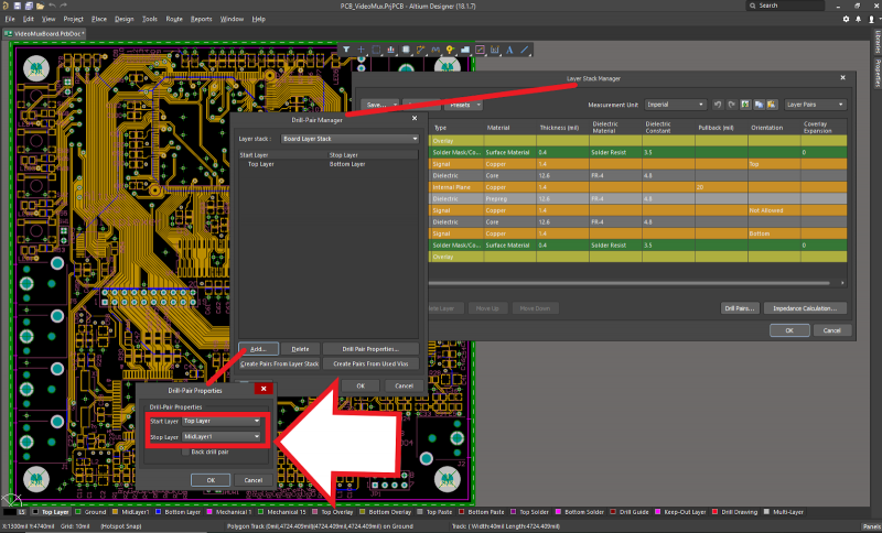
Via design starts when the stackup is being designs. The image below shows where this is done in the layer stack management in Altium; similar tools are available in other commercial CAD programs. First, drill pairs are defined between layers; the default setting for a through-hole via will be to link the top and bottom layers across the entire stackup. If we were using blind or buried vias, we would need to specify a different layer pair where the via would terminate.
Each type of via may be created and defined in the Pad/Via Template Editor and stored within the design’s Local Pad & Via Library. The intelligent Editor recognizes IPC dimensions and assigns names to the custom-made vias that describe their respective IPC definition. This maps to PCB vendor capabilities limits as you define in your design rules. Having access to editors that anticipate your needs and help you create realizable manufacturing constraints while applying customized vias to your design is available in Altium.
Finally, during routing, we can select different via options interactively by looking through out list of pre-made pad/via templates. This is shown below while routing a design. We can see a list of available padstacks within the default library. Each of these padstacks will define a different set of layer pairs, pad sizes, hole sizes, and tenting.

Access via templates during routing.
Backdrilling
When routing high speed signals through vias, there is sometimes concern that backdrilling is needed. This is only important in very high speed channels where bandwidths extend into the 100 GHz range, which will create losses during each via transition. While it is advisable to not route these signals through vias to begin with, if you must route them through vias you should aim to route across the entire stackup. When this is also not possible due to lack of space on a surface layer, backdrilling is used.
Backdrilling is used to remove the leftover stub on a through-hole via when a high speed signal does not traverse the entire PCB stackup. Backdrilling (controlled-depth drilling) is an expensive process that requires excess clearances. These clearances and the tolerance on any leftover stub must be defined in your PCB design rules. This will help ensure your drilling requirements are clearly specified when creating manufacturing documentation.
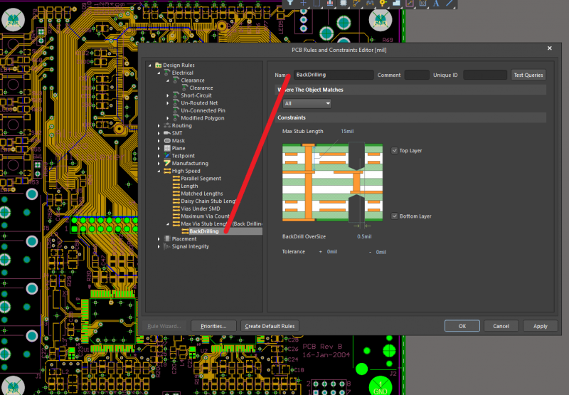
Backdrilling can be applied to specific nets or net classes in your PCB design rules.
Rather than define a new via each time you punch one into your design, you can create a backdrill Net Class and then assign each net that requires backdrilling to that Net Class. You can then assign the backdrill rule to the Net Class, and this will ensure the rule is consistently applied to every PCB via that requires backdrilling.
Via-in-Pad and Via Tenting
Another option to handle high component density designs without using smaller vias is to use via-in-pad with plating (VIPPO) and via tenting. Both mechanisms allow assembly near vias (tenting) or on vias located in SMD pads (via-in-pad). For via-in-pad, be sure to leave at least 4 mil pad size (for Class 2 designs) or 5 mil pad size (for Class 3 designs) to accommodate the required annular ring during drilling. This will help ensure the design is reliable and can be assembled properly.
Prepare Your Design for Manufacturing in Altium
Preparing a design to be manufactured requires generating documentation that includes everything you need for PCB via placement and drilling. Altium will generate this data in your fabrication files with its OutJob feature, as well as all your other standard manufacturing deliverables. Altium also includes utilities to create reports that include a drill table for all of your vias, mounting holes, routed slots, and other features in your PCB. Finally, you can use the Draftsman utility to prepare fabrication drawings that include your layer stack, dimensioned drawings, fabrication notes, a drill table, and much more. You can generate a comprehensive manufacturing file package in Altium and instantly share it with your manufacturer.

Produce drill reports for vias from the PCB editor.
Look no further for an elegant tool that makes it easy to define and configure any type of via for use in your design. Once defined, store the via in your design’s Pad and Via Library for reuse. Access interactive routing and employ via-in-pad and via stitching to manage techniques for delivering a PCB with best-in-class signal integrity. Then configure your design to create drill tables and reports to ensure that your via needs are communicated to the fabrication vendors clearly. With powerful tools at your fingertips, vias are easy to realize in your design.
Altium delivers unprecedented integration to the electronics industry until now relegated to the world of software development, allowing designers to work from home and reach unprecedented levels of efficiency.

