


Ultra-HDI Technology is Not New

At a Glance
A-SAP™ and mSAP have been used in the electronics industry for a long time. Tara Dunn talks about the transition of the semiconductor and super high volume PCB market to medium volume applications. Read now to learn more.


We spend a lot of time talking about these “new” processes. However, these processes are not new at all; they have been used in the electronics industry for a long time. What is new is that this technology has transitioned from the semiconductor and super high-volume PCB market (i.e., smartphones) to mainstream printed circuit board fabricators that can now offer this technology for low to medium-volume applications. It’s about time, isn’t it?
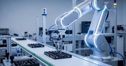
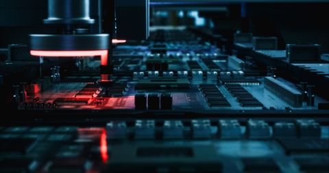
The printed circuit board industry has traditionally been focused on the “subtractive etch” process, and as we all know, that process is typically limited to around 75 (3 mil) micron trace and space, and we have all become pretty adept in doing PCB design within these constraints: HDI, blind and buried vias, micro vias (stacked or staggered), via in-pad plated over design, the list could go on. Printed circuit board fabricators have become skilled at manufacturing these technologies and also at understanding the reliability and producibility challenges associated with high-density-interconnect technology.
I would like to say that this is “comfortable,” but I am afraid my PCB fabrication friends would call me out on that statement. While HDI is a known technology, it is certainly not a simple technology to design or to manufacture.
To start something “new” is “uncomfortable.” It could be a new material combination, starting your first flex circuit, your first rigid flex design, or something much simpler like taking on a new hobby.
What if we remove the label “new” from A-SAP™ (Averatek’s Semi-Additive Process – 10-micron trace/space and above) or mSAP (Modified Semi-Additive Process – 30-micron trace/space and above) technology? I think we can. Let’s look at where the PCB industry is at today:
1. These technologies have been offered by printed circuit board fabricators for a few years, providing experience with both the plating and imaging processes involved. Experience is a wonderful teacher. To shorten the learning curve, work closely with your fabricator when starting a new design with traces at 70 microns or below.
2. The benefits of using ultra-HDI trace and space are easy to understand:
- The overall footprint of the PCB can be reduced
- Routing layers can be reduced
- Multiple lamination requirements can be reduced or even eliminated
- Signal integrity benefits from a more precise process to create traces
- Biocompatibility (we are no longer constrained to copper conductors)
3. There are reliability data available for peel strengths, D-Coupon testing, IST testing, SIR testing, etc.
4. IPC formed an Ultra-HDI Committee in 2020 that is diligently working on an addendum to address areas that may require different specs.
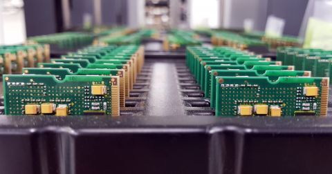
5. Semi-additive PCB processes have been proven with a wide variety of materials, both rigid and flexible circuit materials.
Large DoD Primes and large commercial OEMs are using this technology in their printed circuit designs, and are performing their own reliability testing.
What information do you need to design with ultra-high-density trace and space confidently?
If you are still reading this blog post, I assume you are interested in the benefits of being able to design your printed circuit board with these fine features. To help you achieve your goals, I would like to ask for feedback from the PCB design community:
- What type of information would be most helpful to shorten the learning curve with new PCB design parameters?
- Are there any changes within your Altium design tool that would make this transition easier?
- Do you need additional information on signal integrity benefits? Remember, these benefits are from the semi-additive process, not the trace width. There may be benefits to exploring even a more significant feature size.
- Do you need reliability data? IPC spec information?
- Do you need a tutorial or reference design examples to get you started?
- Would a checklist or design guideline be helpful? What would be key elements to include?
I work with a team of knowledgeable PCB designers using this technology today as well as a strong group of printed circuit board fabricators building this technology. Together, we are committed to providing the PCB design community with tools and resources to explore the benefits of ultra-high-density trace and space. Please comment here or reach out directly. Let us know how we can help!
As a little background for those curious but not familiar with semi-additive PCB process, in our previous blogs we have outlined the basics to SAP processing, looked at some of the top questions related to the printed circuit board stack up, explored some of the “design rules” or “design guidelines” that do not change when designing with these ultra-high-density feature sizes, and explored the design space around the possibility of utilizing these ultra-high density circuit trace widths in the BGA escape regions and wider traces in the routing field. The benefit is a reduction in circuit layers, and the concern is to maintain a 50-ohm impedance. Eric Bogatin recently published a white paper analyzing just this benefit and concern.
About Author
Related Resources
Design to Release, Without the Friction
- Keep reviews tied to the right version
- Reduce handoff confusion and rework
- Spot sourcing and release risk earlier
- Work solo, share when needed
Get Started
Thank you, you are now subscribed to updates.

