A Day in the Life of the PCB Manufacturing Process


Before implementing design for manufacturing, it is important to understand the underlying process behind producing a physical PCB. Regardless of the various technologies present in each facility, a large majority of industry-leading manufacturers follow a specific set of steps to turn your design from a drawing in a CAD application into a physical board.
The standard PCB manufacturing process follows a specific set of steps, and it's up to designers to know and understand all the steps involved in the PCB manufacturing process. By knowing the steps in the manufacturing process, it's much easier to spot PCB design mistakes that create risk of production failures which would require scrapping a board. Every designer must implement design for manufacturing (DFM) steps so that it will be possible to fabricate and assemble a PCB anywhere.
In this article, we'll cover the basics that designers need to know as part of our crash course series on PCB manufacturing. We'll briefly start with the PCB fabrication process that is used to create a bare board. Next, we will examine the PCB assembly process, where components are soldered onto the finished PCB before final test and inspection. Design for assembly (DFA) focuses on design practices that ensure components can be reliably assembled, and just like bare board fabrication, designers have a responsibility to be familiar with the PCB assembly process.
Standard PCB Fabrication Process
PCB fabrication focuses on bare board construction, etching, drilling, and finishing. The table below outlines the standard set of steps used to manufacture multilayer PCBs. This process begins with a complete set of design specifications and initial laminate materials, and it ends with a fabricated board that if fully ready to assemble.
|
|
|
|
|
|
|
|
|
|
|
|
|
|
|
|
|
|
|
|
|
|
|
|
|
|
|
|
|
|
|
|
|
|
|
|
|
|
|
|
|
|
|
|
|
|
|
|
|
|
|
With the final curing of your board complete, a manufacturer will then begin an electrical test process based on the test points you specified in your PCB layout. Electrical testing in the fabrication stage will normally involve continuity testing, where opens and shorts are verified between various nodes called out in your PCB netlist. All boards that pass this verification process are considered complete and are transferred into assembly.
Throughout the PCB fabrication process, there are multiple defects that could occur during production. The most common defects will occur during etching, drilling, and plating steps. Some of the possible fabrication defects that can occur and their possible solutions are listed in the table below.
|
|
|
|
|
|
|
|
|
|
|
|
|
|
|
|
|
|
|
|
|
|
|
|
|
|
|
Once the design has passed fabrication and it has been electrically tested, the board could go through a further battery of tests to ensure quality. This normally involves environmental or mechanical testing to ensure the bare board fabrication process does not damange any materials or etched features in the PCB.
Standard PCB Assembly Process
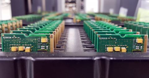
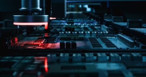
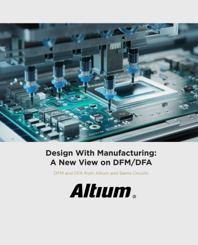
PCB assembly involves placement of components with automated machinery (a pick-and-place machine) and subsequent soldering with an automated process. The main automated techniques for soldering in the PCB assembly process are
- Wave soldering, used with through-hole components
- Reflow soldering, used with SMD components
- Selective soldering, an automated version of hand soldering
Hand soldering is not used in high-volume PCB assembly facilities unless it is aboslutely necessary. The reason for this is the very slow nature of hand soldering, and the varying consistency due to differing skill levels among workers.
After a finished PCB exits the soldering process, it will be inspected with automated equipment, and it will be cleaned of any residues (particularly flux residues) before being packaged and shipped. Completed PCBAsmay also go through their own inspection and testing process to identify any PCBs that would suffer from premature failure. These accelerated life tests involve subjecting a PCBA to extreme heat, pressure, mechanical stress, and electrical stress to determine the operational limits of the device. Once these limits are determined, the processing parameters or the design might be modified to ensure long-term reliability of the design and the final product.

The easiest way to ensure your design will comply with standard DFM/DFA requirements is to take advantage of your PCB design rules. The DRC engine in your design software can be customized around certain rule sets so that you can rest assured your layout will not suffer from common PCB manufacturing defects. Make sure you set DFM/DFA requirements in your design rules before you start your PCB layout.
When you're ready to take a DFM-centric approach to designing your PCB, the process begins with material selection as you start to create your PCB stackup. Material selection can affect DFM in some specialized products, such as high-frequency designs and in high voltage PCBs. Make sure you understand the wealth of material properties for PCB materials and how these affect manufacturing.
- Go to Part 2: DFM in PCB Material Selection
When you're ready to start your design and you want to make sure you meet every DFM requirement, use the design and layout features in Altium Designer®. Once your design is ready for a thorough design review and manufacturing, your team can share and collaborate in real time through the Altium 365™ platform. Design teams can use Altium 365 to share manufacturing data, project files, and design reviews through a secure cloud platform and in Altium Designer.
We have only scratched the surface of what’s possible with Altium Designer on Altium 365. Start your free trial of Altium Designer + Altium 365 today.

