


Design Rule Checking in the PCB Design Workflow


Any time you design a PCB and want to turn it into a real product, you will have to make sure the design obeys the constraints within the standard PCB manufacturing process. This imposes multiple rules on any design, and ECAD software will enforce design rules as you create the board to ensure you obey these important constraints. The ever-increasing complexity of boards has made it nearly impossible to carry out the design rule verification process manually, so designers have to program the right design rules into their CAD software to move easily through the PCB design workflow.
Every PCB will also have some functional requirements, and sometimes, these are at odds with the manufacturability constraints that designers must satisfy. To help ensure you will comply with manufacturability constraints in your PCB, which design rules should you enforce in your software, and how do you resolve conflicts between function and manufacturability? Make sure you enforce the right design rules at the beginning of the PCB design workflow.
Design Rule Checking in the PCB Workflow
DRCs should occur throughout the PCB design workflow, but staying productive is all a matter of how these are triggered. ECAD software includes rules-checking tools that are fully or semi-automated, and designers will need to configure their rules-checking tools at the outset of a new project. Before beginning a PCB layout, a designer should configure rules that fall into the example following categories:
- Minimum clearances between all copper elements and components
- Trace constraints, such as total length, width, routing, etc.
- Layer-specific and net-specific rules, such as rules on differential pairs
- DFA rules related to solder mask, pad sizing, pad-to-pad clearances, and component spacing
- Board, via, and mechanical edge clearances
- Defining net groups that require their own specific groups of design rules
- High-speed design rules relating to signal behavior
All of these design rules will help ensure you comply with most DFM requirements, but managing all these design rule checks in a PCB design manually is a nightmare. It also involves human beings, which always introduces the possibility of error. In addition to a manual design review, once the design is completed, automated rules checking should be performed throughout the PCB design process so that errors can be caught and fixed early.
Automating Your PCB DRC Process
In general, you have three ways to quickly get through rules checking in the typical PCB design workflow.
- Manual design review: The designer and any stakeholders should perform a manual PCB design review to ensure the design satisfies high-level physical and functional requirements. Teams will normally discuss and check specific functional aspects of the design, like mechanical constraints.
- Online PCB DRC: You should always leave this on during the layout and routing phase so that you can ensure your board will satisfy the design rules you define on the front-end. As you're working on the board, any design rule violations will be flashed visually so they can be quickly corrected.
- Comprehensive PCB DRC: Once the design is completed and you're ready to generate outputs, you can run a comprehensive DRC and generate a complete report with any violations. This will check against all the design rules defined in your project, including any rules violations that may have been missed during layout and routing.
Altium Designer contains the industry's best online PCB DRC engine that works as you use your design tools, as well as a comprehensive DRC feature that automatically generates rules violation reports. The breadth of rules that can be defined and checked using the online DRC engine in Altium Designer is also expansive. When you're starting a new project, make sure you define design rules from the list above in the DRC engine.
Defining Design Rules
All design rules surrounding placement, fabrication, assembly, and even electrical functionality can be defined in the PCB Rules and Constraints engine inside Altium Designer. Once you've determined required clearances, trace geometry and routing limits, assembly constraints, and any custom design constraints, you'll want to define these inside the PCB Rules and Constraints Editor window before you begin the PCB layout.
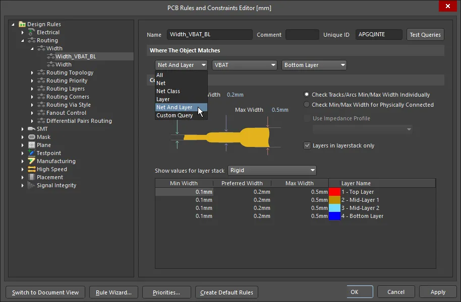
Defining PCB Rules and Constraints in Altium Designer
PCB Design Rule Checker in Altium Designer
When you need to run design rule checks on-demand, you can use the Design Rule Checker in Altium to run a comprehensive set of DRCs in your PCB design. This automates the checking of both logical and physical specifications on your board. The tool allows you to check the design against any or all enabled design rules. Any errors in the design are noted in a report as well as listed in the messages panel. The design rule checker can be run at any time during the design (as well as at completion). In addition, certain rules can be enabled to examine a particular area of the board.
When triggering a DRC with this PCB tool, you can create a report that provides detailed information on any rules violations. The rules violations you'll be able to see include what rule is violated, where the violation occurs, the extent of the violation (e.g., clearances), and the specific components involved by the reference designator. If you want your manual DRC to focus on specific sets of PCB design rules, you can select these in the Design Rule Checker window.

Configuring the Design Rules Checker in Altium Designer
Reports like this are very useful within the PCB design workflow. Internal and external stakeholders may need to access one of these reports in order to determine when a standard rule is okay to violate or when the solution will conflict with functional requirements. Because you can zoom directly to the affected components in the PCB layout, you can then point your manufacturer or CAM department directly to the problem so they can make a DFM determination. This should be done before you send in your board for an independent DFM analysis and report with your fabrication house.
Another Approach: Constraint Manager
There is another feature that some ECAD applications use to create design rules, known as constraint management. These features provide very similar functionality as a design rule list, but the design data may be displayed in a table or list so that design rules can be defined. Design rules are set in three possible categories:
- Physical nets
- Electrical nets
- Clearances
The clearances category is as its name suggests: this involves filling a matrix to define clearances between objects in the PCB layout (pads, fills, traces, etc.). The display is provided on a net-by-net basis, this way the user does not need to write out or click through net-specific queries.
![]()
Physical and electrical constraints are also applied on a net-by-net basis in table format. For each net, the relevant rule category is displayed and the designer can enter values for the relevant constraint category. For example, trace width values can be entered on a net-by-net basis without creating Net Class groups and without writing individual net-based queries to define design rules.

Both approaches will give the same results in design rule checking in a PCB design, where errors are flagged on specific objects falling into each design rule category. Make sure to leverage this important tool as it helps to instantly check important signal integrity, DFM, and DFA requirements inside your PCB design software.
When you’re ready to streamline the standard PCB design workflow with powerful automated tool sets, use the CAD features in Altium Designer® and the built-in design rules engine to make sure your boards will be functional and manufacturable. You and your team will be able to stay productive and collaborate efficiently on advanced electronics designs through the Altium 365 platform. Everything you need to design and produce advanced electronics can be found in one software package.
We have only scratched the surface of what is possible to do with Altium Designer on Altium 365. Start your free trial of Altium Designer + Altium 365 today.

About Author
Related Resources
Table of Contents
Design to Release, Without the Friction
- Keep reviews tied to the right version
- Reduce handoff confusion and rework
- Spot sourcing and release risk earlier
- Work solo, share when needed
Get Started
Thank you, you are now subscribed to updates.


