


A-SAP™ – What do you need to know?

At a Glance
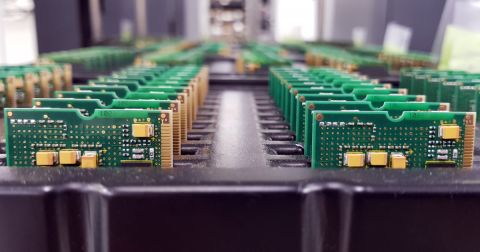
Semi-additive process or SAP allows the ability to design with, and manufacture a 15-micron trace and space repeatedly and reliably. Read more about this great option and opportunity previously not available to PCB designers and PCB fabricators.


The continued miniaturization of both packaging and component size in next-generation electronics is becoming harder and harder to work around and presents a significant challenge for both PCB designers and PCB fabricators.
To effectively navigate the constraints of the traditional subtractive-etch PCB fabrication processes, PCB designs require advanced PCB fabrication capabilities while pushing the limits of finer feature size, higher layer counts, multiple levels of stacked micro vias and increased lamination cycles. When a printed circuit board designer is pushed to design with this level of complexity, this also reduces the supply base of fabricators that are able to meet these needs, further compounding the challenge.
Semi-Additive Processes (SAP) can be implemented and integrated with existing PCB fabrication processes, and provides an alternative that effectively resets the SWaP-C curve while increasing reliability.
The ability to design with and manufacture a 15-micron trace and space repeatedly and reliably provides opportunities previously not available to PCB designers and PCB fabricators. While just scratching the surface, SAP electronics processes can:
- reduce the number of layers needed for routing high-density BGA’s
- increase the hole size
- reduce the number of micro via layers required
- dramatically reduce size, weight and packaging or conversely increase the electronic content within an existing footprint
These benefits and more are being explored and realized as PCB fabricators implement SAP into their PCB manufacturing facilities.
In previous blog posts, we have gone through the basics to SAP processing, recently looked at some of the top questions related to the printed circuit board stack up; and have also explored some of the “design rules” or “design guidelines” that do not change when designing with these ultra-high-density feature sizes.
In this blog post let’s explore the design space around the possibility of utilizing these ultra-high density circuit trace widths in the BGA escape regions and wider traces in the routing field. The benefit is a reduction in circuit layers and the concern is maintaining 50-ohm impedance. Eric Bogatin recently published a white paper analyzing just this benefit and concern.
There is no dispute that narrower traces are going to have higher impedance than the wider 50-ohm traces. The question becomes, if the impedance difference is not too large or the narrower, higher impedance lines are not too long, this may be an acceptable solution. Eric’s paper dives into the questions of what is too large an impedance difference and what is too long. I’ll let you dig into the details but to summarize the conclusion, the impact on signal quality from the narrower region in an otherwise uniform 50-ohm trace interconnect will be from reflections. The impact from its reflections can be at an acceptable level if it is short enough. In the BGA breakout region, it’s possible to use a trace as narrow as half the width of the trace in the routing region and still achieve acceptable return loss to high bandwidth. This condition could reduce the total layer count in the board design and is a useful starting place to consider when narrower traces can be used to reduce the overall layer count.
What are the next steps? The building of test coupons and measurements is underway to prove this out.
Eric and the team are also working on exploring the design space for fine line differential pair transmission lines. Stay tuned, we will link to that once it is published.
The questions about this new capability for fabricators to produce PCB traces and spaces significantly smaller than previously available is churning up many questions. I would ask everyone reading this blog to post their questions or reach out to me directly with the questions. As with any new technology, there is a learning curve, and we are working with a team of people to identify the most burning questions and shorten the learning curve for PCB designers.
To get the thought process started:
- When the aspect ratio for trace height to width is increased, meaning traces are thicker than they are wide, what is the impact?
- Will this higher aspect ratio give us true differential pairs?
- How to you incorporate subtractive etch layers with semi-additive layers?
- Should all layers be thinner layers?
- Can you now use thicker layers?
- How do the answers to the questions above impact the warpage after SMT?
- What happens if you ignore “50-ohm impedance” and use something different?
- What impact will there be on narrow traces if you are also shrinking the length?
- Are there any surface finishes that can not be used with this process?
- How do you design for solder mask coverage?
- What types of materials are compatible with this SAP process?
- Are specific materials required when moving to higher aspect ratio traces?
We need your help to advance this technology and its benefits. There are certainly as many questions as there are answers at this point and I am dedicated to helping answer all of these. I am forming a team of interested and enthusiastic printed circuit board designers to help answer these questions. If you are interested in being part of this team or have questions to add, comment here or reach out to me directly!
About Author
Related Resources
Design to Release, Without the Friction
- Keep reviews tied to the right version
- Reduce handoff confusion and rework
- Spot sourcing and release risk earlier
- Work solo, share when needed
Get Started
Thank you, you are now subscribed to updates.

