


How to Make PCB Gerber Files in Altium Designer Step-by-Step

At a Glance
Looking for the best approach for CAM jobs? Learn how to make PCB Gerber files in Altium Designer from your circuit board layout. Altium's CAM tools can help you quickly create PCB Gerber files.


Once you've got your PCB layout finished and you're ready to start preparing for manufacturing, one of the critical steps is to create PCB Gerber files. These files are used by PCB manufacturers to prepare stencils for photoresist exposure and subsequent etching. When you're ready to create your Gerber files, you need the right set of CAM processor tools that can take data from your PCB layout. Altium Designer helps make the process for generating Gerber files quick and easy without forcing you to use an external program. In this article, we'll guide you through this process of how to make PCB Gerber files and show some example tasks you might need to perform to generate them.
What's in Your PCB Gerber Files?
In an earlier post, we focused on creating a schematic for a simple active amplifier, then we created a simple 1-layer PCB layout from this schematic. The finalized layout is shown in the window below. We only have features in 2 layers on this board (1 silkscreen layer, 1 top PCB layer), as well as vias on some nets.
Finalized op-amp PCB layout with vias and silkscreen visible.
If we want to create Gerber files for this PCB, we need to add a new OutJob file to the project. From here, you can create a host of deliverables for your PCB, including:
- PCB Gerber files in RS-274X and X2 formats
- Bills of materials in PDF or Excel format
- Fabrication drawings
- STEP files for importing your board into a mechanical design program
- Netlists (IPC-D-350 and IPC-D-356)
- DXF/DWG files for the PCB layout
- NC drill files
- Testpoint reports
- IPC-2581 and ODB++ output files
- Pick-and-place files for automated assembly
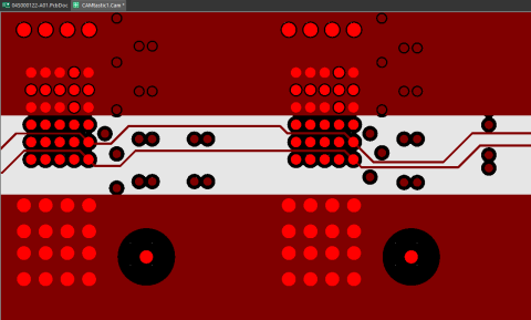
The image below shows the PCB layout above translated into Gerber files and viewed in the CAMtastic viewer. When you create PCB Gerber files, information in each layer will be saved in its own file, and these files can be loaded into a new CAM document for inspection. The image below shows two layers from the above PCB layout. Here, only the silkscreen layer and copper features on the top layer are visible.
A preview of what our final PCB Gerber file will look like.
Note that there are additional files for other layers, which will be generated when you create your Gerber files. These other layers include more information than is shown in the above image. Although they aren't visible above, they include many important pieces of information:
- Pad locations for application of solder paste
- Drill hit locations, which are can be delineated by plated vs. non-plated through-holes
- Information in mechanical layers, such as a drill table, stackup diagram, and any dimensions
- Backdrill layer spans
- Soldermask openings
Some of these documents can be generated quite easily from an OutJob file in Altium Designer, while others require a few steps to setup. However, once you've setup the options in your OutJob file for your project, you can regenerate manufacturing deliverables whenever you want.
How to Make PCB Gerber Files
To get started generating PCB Gerber files, add a new OutJob file to your PCB project. Once this is created, you can start configuring which manufacturing files you need to generate, as well as the file formats you want. The image below shows an OutJob file with multiple options enabled for different sets of manufacturing documentation. An option has been created for Gerber RS-274X files and specifically for backdrilled layers. To create a new export option for Gerber X2 files, right-click in the 'Fabrication Outputs' area and select the Gerber X2 entry.

Use an OutJob file to generate Gerber files.
Note that you can create multiple sets of Gerber outputs. In the above image, the 'Backdrill Gerbers' entry and the 'Gerber Files' entry are both in RS-274X format, but these options will create PCB Gerber files for different layer sets. After you create a new Gerber output option, you'll need to configure what information is exported with each of these options. The image below shows the dialog you'll use to select units, file format, and layers for export. To access this dialog, simply right-click on one of the Gerber file entries and click 'Configure.'

The above image shows the dialog you'll see for the RS-274X format, but you'll see a similar dialog if you want to export in the X2 format. There are two important tabs in this dialog:
- Layers Tab: You can scroll through the table on this tab and select specific layers for export. This includes all the electrical layers on your PCB, as well as mechanical layers, silkscreen layers, and any other layers in the PCB.
- Drill Drawing Tab: From here, you can select which paired drill layers will be converted to a Gerber file. By default, there is a 'Top layer-Bottom layer' option on this tab. However, if you've enabled any other unique via or drill features, like blind/buried vias or backdrilling, you will see options for these layer pairs as well.
In the image below, the PCB Gerber files we want to export, as well as several other manufacturing files, have been enabled and will be exported to your local machine. Simply click 'Generate content' in the highlighted box on the right-hand side of this dialog.

You'll have a complete set of Gerber files and other deliverables once you click 'Generate content' in this dialog.
Now that you've created your PCB Gerber files, you should inspect them to make sure there are no errors. Your Gerber files can reveal some simple problems that can cause a failed fabrication run. If you want to view your exported PCB Gerber files, simply import them into a new CAM document through CAMtastic and scroll through each layer.
Another Way to Create PCB Gerber Files in Altium Designer
If you don't want to create an output job or you don't need to standardize your output format, you can skip this step and create Gerber files from inside the PCB Editor. After saving you PCB layout, you can navigate to ‘File’ > ‘Fabrication Outputs’ > ‘Gerber Files.’ This will bring up the configuration window shown above. You can then select the layers you want to include in your exported Gerber file package, just like you would do with the OutJob file.
You'll notice there are plenty of other fabrication and assembly file outputs that are accessible in the PCB Editor. With Altium Designer®, you can do much more than generate PCB Gerber files. You'll have a complete set of CAD tools needed for PCB layout, routing, and fabrication/assembly drawing creation in a single program. Once you've finished creating your PCB layout and manufacturing files, you can easily share your data with your manufacturer using the Altium 365 platform.
We have only scratched the surface of what is possible to do with Altium Designer on Altium 365. If you want to learn more on how to make PCB Gerber files ore more information on CAM jobs, you can check the product page for a more in-depth feature description of the software or one of the On-Demand Webinars.

About Author
Related Resources
Related Technical Documentation
Table of Contents
Design to Release, Without the Friction
- Keep reviews tied to the right version
- Reduce handoff confusion and rework
- Spot sourcing and release risk earlier
- Work solo, share when needed
Get Started
Thank you, you are now subscribed to updates.


