


How to Create a PCB Schematic in Altium Designer

At a Glance
Looking for the best schematic designer? Learn how to make a schematic like a professional in Altium Designer with steps to add components, grounding, and more.


There’s an important step in creating your PCB layout: How to make a schematic? You might feel overwhelmed with all of the options, but don’t worry! Whether you’ve got decades of experience in your pocket or just starting your design or engineering career, your PCB design begins with schematic capture. Below is a schematic capture tutorial in Altium Designer, covering everything from component access to wiring parts together into circuits.
A PCB Schematic Tutorial in Altium Designer for a Basic Audio Amplifier
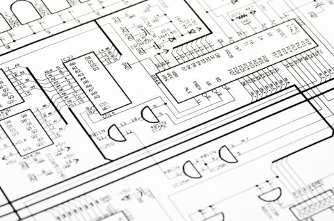
If you’re still learning, it’s best to work with a relatively simple circuit. I’ve chosen to base this work on a very simple amp using the LM386 IC. This component is designed for audio reproduction in low-power devices, plus it is quite easy to work with a schematic editor. To give you a picture of what we’ll end up with, the image below shows our finished schematic:
Finished schematic for a simple audio amplifier in Altium Designer.
With this finished schematic in mind, let’s look at how you can move from an idea to a complete PCB schematic in this Altium tutorial.
Step 1: Open a New Schematic
The first step is to create a new PCB project if you haven’t done so already. To create a new project, click File > New > Project > PCB Project. This will create a blank project in your workspace, which is displayed in the Projects panel. From here, you can add existing files to your new project, or you can create blank files for your new board.
Once opened up, you’ll need to create a new schematic file. You can right-click on the new PCB Project in the Projects panel, and navigate to Add New to Project > Schematic. This will open up the Schematic Editor window, and you’ll see a blank schematic. If you haven’t done so already, you’ll need to add component libraries to Altium Designer. Otherwise, you can skip to Step 3.
Step 2: Access Component Libraries
Altium Designer comes with multiple component libraries included with your installation and accessible through the cloud.
- Celestial library - This library is accessible in-app and includes access to a huge collection of open-source component components maintained by the design community. To create your own variant, you can clone the library here.
- File-based libraries - Users with an earlier installation of Altium Designer, or who have components in library files, can install libraries into Altium Designer. Installed libraries will be accessible from the Components panel.
- Manufacturer Part Search panel - This resource contains CAD data and supply chain information provided by manufacturers and by Octopart. CAD models can be searched and instantly downloaded into a PCB project.
Since we’ll be using a common LM386 op amp, we can access this from the Texas Instruments Amplifiers.IntLib, Miscellaneous Devices.IntLib, and Simulations Special Function.IntLib libraries. If you don’t have the Texas Instruments component libraries on your local machine, you can find the parts you need from the Manufacturer Part Search panel. This will download the component data directly to your Library folder and will automatically add the component library into Altium Designer.

An LM386 op-amp can be located in the Manufacturer Part Search panel in Altium Designer.
Step 3: Add Central Components
One strategy to make a schematic for printed circuit boards is to centrally locate the most important ICs in your schematic. Here, we’re building a new schematic specifically around the LM386 op amp, and the remaining components required for the amp will be arranged around this. If you search “LM386” in the library's search bar, you’ll find a few options. I simply selected the first part (LM386M-1) as a starting part.
LM386 was placed in our new schematic.
Once you place this component, you’ll need to give it a reference designator. I’ve labeled component U1, which is the standard designator format for integrated circuits. To edit the values of the IC, simply double-click on the value you’d like to edit directly in the schematic. You can also click on the component and open the Properties panel.

Schematic with central IC component showing component properties.
Once we’ve added the appropriate part and designator, we can move on to placing other components.
Step 4: Add Other Components to Your Schematic
Similar to Step 3, we’ll be searching the library database for our basic reference components (caps, resistors, battery sources, speakers) to place around the IC. Instead of searching through the Texas Instruments library, however, I simply used the Miscellaneous Devices.IntLib library to find the other components I needed to complete my circuit. Working with this library is quite useful as you can place passives with any values you like and import your circuit into SPICE simulations. This is an important part of circuit design and helps you examine the functionality of your device before you begin your layout.
For purposes of this amplifier design exercise, I’ve arranged the remaining components as shown below:

Schematic with another component around the LM386 op-amp.
After you’ve placed all the components on the board, you can begin connecting them to neighboring components.
Step 5: Add Ports, Power, and Ground
In many designs, you’ll likely need to place an object that references a data input or a data output. This can be used to designate a connection to a different PCB schematic or another board as part of a multi-board project. For the purpose of this amplifier, I need to note where the audio input will come from. Instead of trying to leave a bunch of sticky notes on where to place the audio input, I simply add a port to the schematic to denote this information. To place a port, navigate to the upper toolbar and select ‘Place Port’ to place this reference into the schematic in the same fashion as any other component.
You can change the text to whatever you like, but it’s best to write something that directly describes the functionality of the port, or where it will connect to. I’ve shown this in the image below.
Schematic noting the reference audio port placed on the left-hand side.
In addition to ports, you’ll need to add any power and ground connections needed in your printed circuit board. In this device, power is provided by a battery, so we don't need to add a power connection. In other devices, you may need a power port, which can be added from the top toolbar in the Schematic Editor. You can add grounds by selecting the standard GND symbol from the upper toolbar. You can connect all the ground connections to the same point, or you can add a GND symbol to each ground point. Remember that your PCB schematic is not a literal reflection of your layout. In other words, you will be able to route to different ground points in your layout, even if you placed a single ground point in your schematic.
In order to keep things organized and keep yourself from crossing a large number of lines in your PCB schematic, it’s usually easiest to just place a GND symbol on each ground point in the schematic. This is shown in the image below.

Added grounds on schematic attached to necessary components.
Step 6: Making Connections
We’ve arrived at the last step required to get the schematic capture. Here you’ll need to route connections between components; navigate to the upper toolbar and select the ‘Place Wire’ tool. From here, all you need to do is click the pin where you need to start the wire, then the pin to end the wire. In this particular example, since we’re working on a pre-established design and know which components need to be connected to each other, the wiring should be straightforward.
If you’ve been following along with this schematic capture tutorial, your schematic should look similar to the schematic shown below.

Finished schematic tutorial in Altium Designer.
Congratulations, you’ve just learned how to make a PCB schematic in Altium Designer tutorial! Give yourself a pat on the back as you’ve taken the first step towards printed circuit board greatness. Save your schematic and your PCB project under any name you like. The next step is to import your design into a blank PCB layout. Take a look at this article to learn more about starting your new PCB layout.
If you’re looking for more resources to help you make a schematic capture, take a look at the following articles:
- Altium Designer Documentation
- Schematic Placement and Editing Techniques
- Creating Connectivity
- Design Reuse with Managed Schematic Sheets
If you’ve enjoyed this tutorial on how to make a schematic with Altium Designer and you’re looking to expand your knowledge even further, check out more great resources from our PCB Design Blog, or talk to an Altium Designer expert today.
Whether you're new to Altium Designer or just upgraded your PCB design software to Altium Designer after years of working in OrCAD, PADS, or another design program, a good schematic capture is critical for PCB design. Although there are always challenges with new projects and software, Altium Designer’s unified design environment streamlines every step of design and layout to make up for it.
We have only scratched the surface of what is possible to do with Altium Designer on Altium 365. You can check the product page for a more in-depth feature description on PCB designers or one of the On-Demand Webinars.

About Author
Related Resources
Related Technical Documentation
Table of Contents
Design to Release, Without the Friction
- Keep reviews tied to the right version
- Reduce handoff confusion and rework
- Spot sourcing and release risk earlier
- Work solo, share when needed
Get Started
Thank you, you are now subscribed to updates.

