How to Prepare Your PCB for Outgassing in Ultra-High Vacuum Systems

No PCB material is perfect, and this statement particularly applies to materials used to build PCBs. The materials used in a PCB stackup are composite laminates containing a fiberglass weave and a resin filler. The resin contains a wealth of organic compounds and volatile materials that can undergo outgassing. There is always some small amount of outgassing, but under certain conditions, the rate of outgassing will increase. This is a phenomenon that occurs in high vacuum environments and can hinder or ruin nearby instruments.
If you’re designing PCBs for ultra-high vacuum (UHV), or boards that will be thermally cycled, you will need to determine how to reduce PCB outgassing. In an ideal world, we would be able to eliminate outgassing, but in reality you can only reduce or suppress outgassing from a finished product. Application areas like space, electro-optics, and precision instrumentation all rely on low outgassing, especially when devices are deployed in a harsh environment.
What is PCB Outgassing and Why Does It Matter?
Outgassing (or offgassing) occurs when gassed trapped in a material undergo mass transfer to the surface of the material and are drawn into the external environment. It is a natural process that is related to three fundamental mass transfer mechanisms:
- Diffusion, where transport of volatiles inside the laminate is driven by a concentration gradient
- Desorption, where volatiles are desorbed from surface sites in a material
- Vaporization, where volatiles are emitted due to a phase change into the gaseous phase
In ambient conditions, the main mechanisms by which outgassing occurs are diffusion and desorption. Changes in the surrounding environment will change the outgassing rate, such as changes in temperature or the environmental pressure where the board is being operated. This leads to three common instances where outgassing is likely to occur during operation: during wave/reflow soldering, in high vacuum, and when running at elevated temperature.
Outgassing During Soldering
When a PCB is put through an automated soldering process, specifically wave or reflow, there will be some outgassing. During the process, the board will be brought up to elevated temperature, either by the high heat of the molten solder or the high heat of the oven. During the thermal excursion to high temperature, the PCB will begin releasing trapped gases and moisture, primarily from the bulk of the PCB laminate.

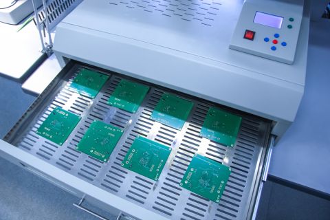
The solution here is to pre-bake the bare PCB before soldering. The typical pre-bake temperature is from 100-120 °C or higher, and this may be done in vacuum when the end devices is targeting an aerospace application, as described below. By pre-baking the board, you are removing residual moisture from the bulk PCB material.
Outgassing in High Vacuum
Outgassing can also happen in vacuum, even if the board is not at an elevated temperature. The reason for this is that diffusion rates are temperature dependent and pressure dependent. So if the pressure in the surrounding environment drops, diffusive flux of volatiles will be higher because there is no air pressure that can block diffusion. In addition, vaporization can occur when the vacuum is high enough. This is typically a problem that occurs in systems operating in space, both in pressurized (spacecraft) and un-pressurized systems (satellites).
Outgassing at High Temperature
When a board that contains residual moisture and other volatiles is brought to higher temperature, the outgassing rate will increase. When brought above the boiling point of water, moisture trapped in the bulk of the PCB laminate material will migrate towards the surface and vaporize, thus the outgassing rate increases. The outgassing will continue until the PCB is brought to a lower temperature or until the moisture content in the PCB is depleted. This should explain why it is recommended to bake PCBs before assembly in a wave or reflow process; the pre-bake process will force removal of volatiles from the PCB material (see below for more information).

Note that some systems can experience extremes of thermal cycles and run at high vacuum, e.g., equipment deployed in space. Electronics used in satellites, for example, are only somewhat protected thermally, but modern satellites are not sealed or pressurized. As a result, they come to a rough vacuum very quickly when placed into orbit, and the enclosure will eventually settle to a high vacuum environment.
Why Outgassing is a Problem
Outgassing can be a big problem in circuit boards because PCB materials are porous composites, and they tend to trap gases and moisture during the fabrication process. The problem with outgassing is that the desorbed/vaporized volatiles can condense on a cold surface and they become a contaminant. This causes multiple problems in systems used for precision measurement, imaging, sensors, and chemical analysis. In unmanned systems, this is a problem because there will not be any human around to maintain the system and remove contaminants. One of the simplest
One important point to note is that outgassing occurs from other surfaces and materials besides the PCB. When the PCB is implemented into a larger system, there will be an enclosure, cabling and wires, and specialty materials like thermal compounds or shielding compounds. Any of these other materials can exhibit outgassing. When brought into vacuum, outgassing will alsway be higher as desorption and diffusion rates are higher, and vaporization will occur as well. All of these materials
How to Suppress Outgassing
There are some simple design and production steps that can help reduce outgassing from a PCB and other materials used in the assembly. These are listed in the following table:
|
|
|
|
|
|
|
|
|
|
|
|
|
|
|
|
|
|
Manufacturers bake their printed circuit board for one purpose that serves a variety of ends: to remove moisture. Water trapped in circuit board materials can desorb or vaporize and outgas during reflow soldering, wave soldering, temperature cycling, and operation in vacuum. Pre-baking attempts to remove volatilized compounds in the interior of the PCB laminate, with a specific focus on excess moisture. If the PCB will be deployed in a vacuum environment, then you’ll need to pre-bake your PCB in a high vacuum. This will help ensure there is as little residual moisture as possible, as well as minimal concentration of any other volatiles trapped in the PCB laminate.
Choosing the right printed circuit board materials is key when trying to reduce outgassing. If you need low outgassing materials for your PCB, products like Rogers Corporation’s RT/duroid series. Flexible circuits materials (Kapton) also exhibit low outgassing. You should also start your build by talking to your manufacturer about using a vacuum pre-bake process to remove as much volatiles as possible from your boards.
Outgassing Standards and Guidance
There are three commonly cited standards describing outgassing test procedures and performance requirements. These include:
- IPC-1601 - This standard specifies a baking process that targets removal of most contaminants that can become trapped in epoxy-fiberglass composites. The standard requires baking a bare PCB in the 100 to 125 °C temperature range.
- SP-R-0022A - This NASA standard lists acceptable limits on outgassing from material sets used in PCBs that will be deployed in space. There is also a testing procedure listed in this standard.
- ASTM E595-07 - This standard from ASTM International (formerly known as American Society for Testing and Materials) defines a test procedure for direct measurement of volatile outgassing from PCB materials.
Most fabrication houses will default to the IPC standard whenever a pre-bake is requested. If there is an industry standard that applies to your product, make sure you request it be followed by your assembly house. This can be specified in your board's assembly notes.
More guidance from NASA on designing for reliability and outgassing can be found in these resources:
- High Voltage Engineering Techniques For Space Applications
- Vacuum Stability Requirements of Polymeric Material for Spacecraft Application
- Thermal Interface Materials (TIMs) and Challenges Faced by TIM Suppliers
Note that even if you pre-bake your PCB, you will not totally protect your board from moisture reuptake. Water can still adsorb onto surfaces that have been baked a pre-treated; the same applies to treated boards with an applied conformal coating. Therefore, whenever the board is exposed to air, there will always be some small amount of residual moisture, which will then desorb at high temperature/pressure.
When you need to design high-reliability electronics for your next product, use the complete set of CAD features in Altium Designer® to build your most advanced devices. When you’ve finished your design, and you want to release files to your manufacturer, the Altium 365™ platform makes it easy to collaborate and share your projects.
We have only scratched the surface of what’s possible with Altium Designer on Altium 365. Start your free trial of Altium Designer + Altium 365 today.

About Author
Related Resources


Related Technical Documentation


Table of Contents
Connect design data and requirements for faster design with fewer errors
Request access to Altium 365 Requirements Manager!
Accelerate your design process for faster time to market
Analyze requirement change impact for thorough resolution
Automate risk assessment and compliance
Efficiently reuse requirements, components, and connections
Create accountability and reduce intent miscommunication
Request Access
Thank you, you are now subscribed to updates.