


Picking the Right Bluetooth Antenna Types for Your PCB Design
Have you ever tried tracing your wireless usage? Bluetooth PCB antenna design has gotten our bluetooth electronics everywhere by allowing devices to connect to a standardized matching network. For instance, I am streaming music from my phone to wireless headphones. Later, I’ll hop into my car and take phone calls through my hands-free computer system. Then I can get home and talk to my home-assistants to tell me the weather, set dinner timers, take off my shoes, give me a massage… Oh, I got ahead of myself there.
Bluetooth-enabled devices have a myriad of applications ranging from healthcare, internet of things, entertainment, and VR. Creative designers have a number of options for including Bluetooth antennae in their PCB. Custom-designed antennas are becoming more popular, and chip antennas are currently at record low costs. What’s stopping you from jumping into your own Bluetooth antenna designs?
Narrow Down Your Device Requirements
Even if you have no RF design experience, you will need to learn to think like an RF designer. The first step in choosing an appropriate Bluetooth antenna for your PCB is to narrowly define the functional requirements of your device. Ask yourself the following questions:
- Is your product flexible or wearable?
- What are your form factor constraints?
- Is your product mounted on or packaged in metal?
- What is your required communication range and antenna gain?
Once you have narrowed down your requirements based on these questions, you are one step closer to choosing the right Bluetooth antenna for your device.
If your product is wearable, it probably also has a small amount of available real estate, and a microstrip or chip antenna is desirable. If the most important requirement is long-range communication, a metal plate antenna may be the best choice to achieve appropriate antenna gain. Optimizing your functional design requirements like a non-signal-interfering PCB trace layout within the above framework will ensure that you pick the best antenna for your device.
Ceramic Chip Antennas
A prepackaged ceramic chip antenna has very small form factor at the cost of low gain and efficiency. Their moderate bandwidth and cost may not make them the best option for applications like ranging or location-tracking. These chips are desirable in rigid wearable devices that typically operate in low-range applications.
There are a number of manufacturers that produce different chip antennas. This gives designers considerable flexibility in selecting the best bandwidth, gain, and form factor for their Bluetooth-enabled devices.
Placing a chip antenna on a PCB is also quite straightforward and does not require many design rules or simulations. The chip should be not placed over a ground plane in order to suppress susceptibility to EMI. Any signal traces, especially traces with vias, will need to be impedance matched with an inductor and capacitor pair. This will reduce insertion loss and prevent signal reflections.
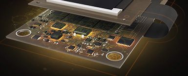
Bluetooth-enabled PCB module
Metal Plate Antennas
Metal plate antennas have high-efficiency, linear gain, and can handle large amounts of power, as well as low bandwidth. They also have high cost and a large footprint, and they may not be ideal in applications requiring smaller form factors. These antennas operate with linearly polarized radiation and can be designed as a monopole, dipole, or inverted-F antenna.
As its name implies, these antennas are formed from a metal plate that has a specific pattern cut into the plate. A metal plate antenna is not directly mounted on the PCB. Instead, this antenna sits above the board and contains a right-angle bracket that provides the antenna to the remaining electronics. The space below the antenna should be cleared of grounding planes, power planes, and other components.
The metal plate antenna is placed at one edge of the PCB, usually in the corner of the board. As odd as it may sound, the spacing between the edges determines the resonance frequency of the antenna in addition to the geometry of the antenna itself. Increasing the spacing between the edge of the board and the edge of the antenna increases the resonance frequency and the bandwidth.
Microstrip Antennas
If your form factor will not accommodate a plate antenna and costs are a critical issue, you might opt to place a microstrip antenna on your PCB. These antennas have better linear gain and efficiency than a chip antenna. They also have higher bandwidth than a plate antenna and are easier to manufacture as they can be printed directly onto the PCB.
Designing a microstrip antenna requires a precise layout during the design phase. Slight deviations in the dimensions of the microstrip can change the resonant frequency of the antenna, and this leads to a decrease in linear gain and efficiency at 2.4 GHz for larger resonance shifts. This will also cause a decrease in the communication range. Your manufacturer must be able to accommodate the tight tolerances of these antennas.
Various microstrip geometries can be used to build Bluetooth antennas. The L-shaped, inverted F, and bow-shaped antennas are all popular designs. These antennas all transmit and receive linearly polarized radiation at 2.4 GHz and have smaller form factors than a plate antenna.
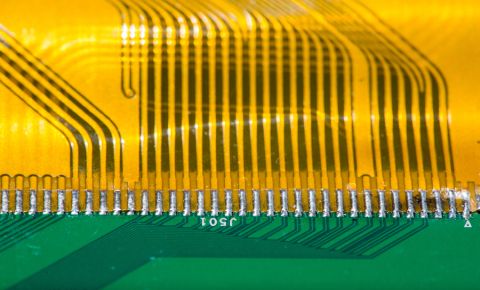
Strip antenna in an RFID tag
A diamond-shaped plate-like antenna is also a popular Bluetooth antenna design that uses circularly polarized radiation. This antenna has a larger footprint on the PCB and requires an impedance matching net, but it also has better sensitivity to linearly polarized RF radiation. Getting the resonance frequency just right also requires matching the microstrip dimensions with the dielectric constant of the substrate.
Using a PCB substrate with a higher dielectric constant will enable smaller circuit features and allow reduced antenna size for a given frequency. Choosing substrate and microstrip materials with matching volumetric expansion coefficients is important for devices that will be used over a broad temperature range, as this will help prevent fracture or delamination.
PCB layout software like Altium Designer makes it easy to design intelligent your Bluetooth-enabled device, so there's no excuse not to get on the matching network shared by so many other devices. To learn more about Altium Designer and how its built-in tools can help you add Bluetooth capabilities to your new product, talk to an Altium Designer expert today.
Related Resources
Related Technical Documentation
Table of Contents
Altium is transforming the electronics industry so thoroughly that our web pages need a minute to catch up. For a short time, some information on this page may be outdated.
We appreciate your patience. It will be worth the wait!
Learn More
Thank you, you are now subscribed to updates.