How to Avoid Common PCB Signal Integrity Issues in Your Designs

Over the years, I've been asked to build a range of different circuit boards, each with different challenges in the core design approach. I've also had to rework boards that had some common signal integrity problems, which would often lead to EMC failure or link failure. The common failure modes I have encountered in reworked boards are interface failure (high BER or inability to read/transmit data), excessive radiated emissions, excessive crosstalk, and repeated system restart, all of which are related to some common signal integrity problems.
For new designers, there are some simple stackup design, layout, and routing practices that will eliminate 80% of signal integrity problems on 80% of high-speed PCBs. Not all PCBs will be running at extreme speeds with extremely fast signals and edge rates, but even if you only have a few high speed interfaces and serial buses, these PCB signal integrity can help you be successful.
What Problems We Want to Solve
The entire reason high-speed PCB designs are more prone to signal integrity failures today compared to the past is because edge rates in modern components are much faster. If we drill down from the common EMI problems to the root causes of these system-level failures or compliance failures, there are a few common signal integrity problems that are related to these problems:
- Reflections in interfaces without an impedance specification
- Excessive crosstalk in parallel traces
- Switching noise on outputs from integrated circuits (ground bounce and supply bounce)
- Radiated emissions when crossing reference planes or routing onto cables
Reflections and Impedance
In the past, before impedance calculators were convenient to access and widely accessible, impedance would need to be measured or calculated with a specialized computer program. You could also do it by hand with a calculator if you know the right formula to use. This might result in an awkward trace width that was difficult to implement in tapeout. As a result, it was convenient to get the impedance close enough to specification, and then you would try to keep the trace short enough to ensure there was minimal input impedance deviation. At that time in the past, most digital designers probably did not concern themselves with concepts like "input impedance deviation" and it is the reason so many older guides focus on an outdated "critical length" design rule.
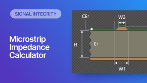
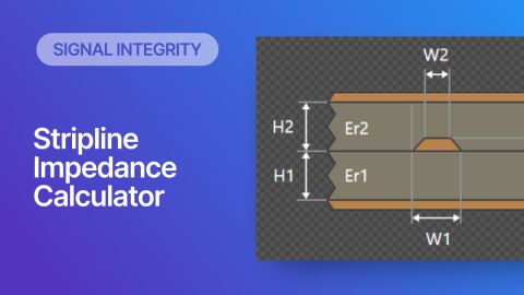
What's important to note is that modern PCBs with impedance-specified buses should always be designed with trace impedance matching the interface specification. It's extremely easy to do this in today's designs, especially with today's impedance calculators available. This must be performed during the initial stage of the PCB layout, when the stackup is designed and layer assignments are determined.

Crosstalk
When crosstalk occurs between two nets, a pulse of current will appear on a victim net whenever a signal switches on an aggressor net. The resulting crosstalk can be measured both at the driver end and the receiver end of the victim net. There are
- Route digital signals on top of a ground plane and between ground planes
- If you're not sure how far apart to space your traces, use the 3W rule as a conservative estimate
- If you bring ground very close to the traces on the next layer, you may be able to use less than 3W spacing (see below)
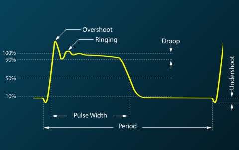
Top: switching digital signal with minor ringing (could be due to reflection, ground bounce, or both). Bottom: crosstalk excited in a neighboring line during the signal's switching events.
What you should not do is use a guard trace unless you understand specifically how different types of guard traces affect crosstalk. Depending on the termination type and routing layer (crosstalk or stripline), guard traces can increase crosstalk rather than decrease it.
When you have very thin dielectric layers in the stackup, you can often violate the 3W rule for a given crosstalk target and you could place traces closer together for a given crosstalk target. However, make sure to simulate this in the time domain with a pulse response, or you should simulate the multi-port S-parameters for the two traces. The exact same ideas apply to crosstalk between differential pairs, although in this case the spacing between the pairs is also important for suppressing differential crosstalk.
Switching Noise
Faster edge rates in legacy designs, using the same frequency and trace length as in earlier generations of integrated circuit technology, can now produce ringing observed on the outputs from an integrated circuit, known as ground bounce. When many I/Os switch simultaneously and produce this noise, it is more often called simultaneous switching noise. Noise will also appear on the power rails during switching events, which is sometimes called supply bounce.
Both factors relate to inductance along the current path in the power delivery network (for supply bounce) and the path to ground along an I/O buffer (for ground bounce). The problem is overcome with use of sufficient capacitance; for supply bounce this requries selection of enough capacitance on the power rail with progressively higher self-resonant frequencies to overcome inductance (ESL), while for ground bounce this requires placing small capacitors on I/O supplies on the digital IC.
Many of the processors where you are likely to observe this will be in BGA packages. These packages allow placement of the required capacitors and routing techniques that will help reduce the inductance that causes ground bounce. Aside from selecting the proper capacitors for a design to provide stable power and signal excitation, there are two other important giudelines that happen in the PCB layout:
- Route each pin on the digital component to ground with its own via, rather than ganging up connections onto single vias.
- Place the capacitors as close as possible to the supply/ground pin pair. This is very easy on BGAs as the back side can be used.

These are signal integrity problems, but supply bounce is also a power integrity problem. Because signal integrity and power integrity issues tend to manifest themselves as intermittent operation, they may be rather difficult to diagnose. It’s always better to find these issues during the high speed design process, and eliminate them at their source rather than attempting to resolve them at a later stage leading to delayed production. With the help of a stackup planner tool, it becomes much easier to implement solutions for signal integrity issues in your designs.
Excessive Emissions
The points above all relate to emission of electromagnetic radiation from the PCB. Some of this radiation exists or is received in the PCB (in the case of crosstalk), while some of this radiation is emitted away from the PCB. It does not take much radiation to fail EMC compliance testing, which will be required for products placed into market at high volume.
The first place to start ensuring signal integrity in your board build is to create a high-speed PCB stackup that can support impedance and low noise. The stackup is the most critical component of the assembly, and its specifications need to be planned carefully to prevent impedance discontinuities, noise, and excessive electromagnetic emissions. When looking at your board stackup, keep these tips and recommendations in mind for your next design:
- All signal layers should be adjacent to an uninterrupted reference plane, which creates a clear return path and eliminates broadside crosstalk.

- Place large power rails on a layer that is also adjacent to a ground plane in order to reduce AC impedance in the PDN. Closely coupled planes reduce AC impedance at the top end and dramatically reduce electromagnetic radiation.
- It is often advantageous to route high-speed signals between planes to reduce radiation.
- Reducing the dielectric height will result in a large reduction in your crosstalk and radiated emissions without reducing available space on your board.
- Understand how to design stackups under two different approaches: controlled dielectric and controlled impedance.
Routing and Workflows
After carefully planning your stackup, it’s now time to move onto the routing of your board. With careful configuration of your design rules and workspace, you’ll be well equipped to successfully route your board in the most efficient way possible. Use these tips to make routing your board easier while avoiding unnecessary crosstalk, radiation, and signal quality issues.
Although chips, PCBs, and substrates will continue to become more advanced, the basic building blocks of signal integrity still have not changed, and these guidelines will set designers up for success going into the future. Whenever you need to design PCBs while ensuring signal integrity, make sure you use the complete set of PCB design features and world-class CAD tools in Altium Designer®. To implement collaboration in today’s cross-disciplinary environment, innovative companies are using the Altium 365™ platform to easily share design data and put projects into manufacturing.
We have only scratched the surface of what’s possible with Altium Designer on Altium 365. Start your free trial of Altium Designer + Altium 365 today.


