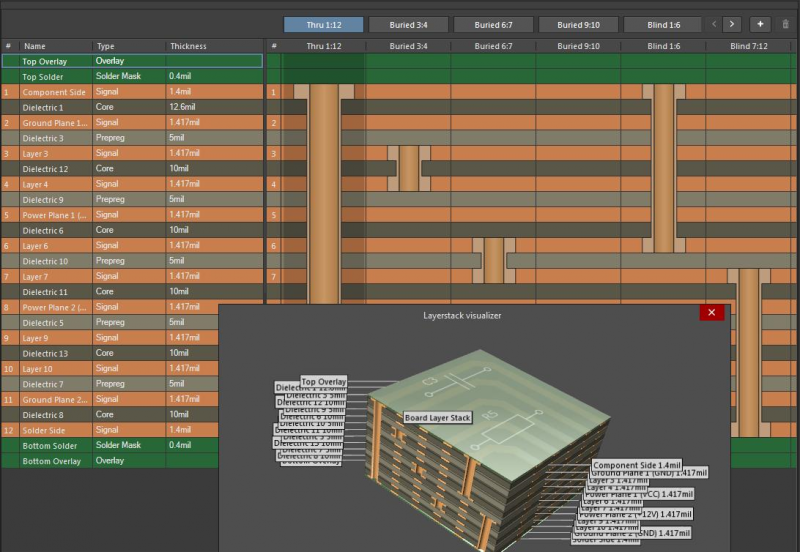
Multi-Layer PCBs & Layer Stackup
Browse our library of resources to learn more about multi-layer PCB design & layer stackup.
Filter
found
Sort by
Browse our library of resources to learn more about multi-layer PCB design & layer stackup.