


How to Design and Fabricate the Best 4 Layer PCB Stackup with Altium Designer


Among multi-layer stackups, four-layer stackups are probably the most common type of PCB stackup. Four-layer stackups allow for high-speed routing, integration of high power, and multiple signal layers where needed. In instances where routing islands need to be carved out above different ground or power regions in the PCB, four-layer stackups give you enough space with ground planes to implement such strategies.
Although four-layer PCB stackups are entry-level stackups, it is very common to see newer designers choose the wrong type of four-layer stackup. There are a few very common mistakes that are made with these stackups:
- Perception that a power plane is required
- Filling with copper pour when it is not needed
- Cutting up grounds on internal layers
- Facing grounds on the component layer when not necessary
To help designers scale up their layer count as needed, we compiled our best set of resources on the different types of four-layer stackups and PCB design. This guide will help you select the right stackup and get the required fabrication information from your fabrication house. Getting these steps correct with a four-layer stackup helps ensure success as you move to higher layer counts.
Types of Four-Layer PCB Stackups
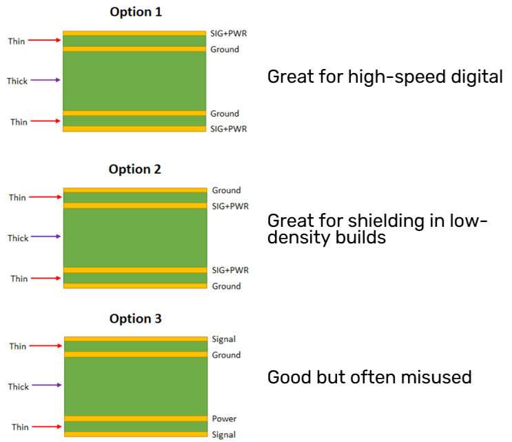
There's at least a dozen ways to arrange layers in a four-layer stackup, but there are three types of four-layer stackups that are most common. These most common four-layer stackups recognize the fact that planes are being used, which is one of the main reasons to start using four-layer stackups. The three most common approaches to four-layer stackups are shown in the graphic below.
Click the links below to learn more about:
These stackups all have some common characteristics, which are related to how four-layer stackups are produced by manufacturers:
- They have a thick core layer and thin outer prepreg layers
- The core layer is normally copper clad so that it can be easily used to form planes
- The outer layers are almost never HDI build-up layers
- The core and prepreg materials could have any Tg value
- The materials could be low-loss FR4 or PTFE laminates
Given this information, many new designers will take a crack at creating their own stackup from a mix of materials. Four-layer PCBs are a good entry-level stackup to start designing from common materials. If you don't need a controlled impedance build and any dielectric constant value would be acceptable, you can search online for material options and start creating your own stackup design. I will discuss this more below.
Using Each Layer in the Common Four-Layer Stackups
Signal and ground as they are placed together in the four-layer stackup shown above allow for these PCBs to be used for many high-speed digital systems. When a ground plane is placed next to a signal layer, it is possible to design traces to have specific impedance values, which is based on the trace width and the layer thickness. This is a requirement for most high-speed digital interfaces which are faster than SPI.
Digital interfaces that can be easily supported on a four-layer PCB stackup include SDRAM, DDR, USB, HDMI, LVDS, and Ethernet. These interfaces require traces to have specific impedance (either single-ended or differential or both). To size the traces appropriately, the dielectric thickness is adjusted; thinner layers give a narrower trace in order to hit the impedance requirement.

There is still another point to discuss, which is the usage of a power layer in a four-layer stackup. I think this is a less common type of board, and the power plane is often used in situations where it is not needed. However, you can certainly use a power plane for the convenience of routing if you like, as long as other conditions are met. Take a look at the resource below to learn how to do this properly.
An Alternative Four-Layer PCB Stackup Approach
The three-layer stackups shown above are arguably the most common. The last one shown above, where a layer is dedicated to power, is often the most misused by new designers. Still, there are four-layer designs that integrate digital and a power plane into the same stackup, and there are alternative approaches with stackups that deliver very good performance.
One example is the stackup shown below, which I have discussed in a video on the Altium Academy YouTube channel. In this stackup, a dedicated power layer is used with a single signal layer on the surface. The other two intervening layers are ground planes.
I like this stackup for certain types of builds where component density is not too high, but there will be nodes in the design where circuits are switching at high current with fast edge rates. This creates the possibility for strong radiated emissions, but sandwiching the power layer between ground planes helps to suppress noise from these circuits. A good example of a system that could use this stackup is a power system with a small digital section for monitoring power and communicating with an external device.
Note that the power layer does not have to be a complete plane; it can be composed of multiple large rails and even some traces for signals.
Standard Four-Layer Stackups from Manufacturers
PCB fabrication houses have standard stackups they will use for many builds, including four-layer PCBs. The four-layer stackup you find on a fabricator's website could be standard thickness at 1.57 mm, although other common thickness values are available, such as 1 mm or 2 mm. If your design does not have strict material requirements, then the fabricator will use their standard stackup.
Typically, the standard stackups will be specified in a table such as that shown below. They will generally provide layer thickness and dielectric constant at a minimum, as well as two options for Tg values. An example from Worthington Assembly's website is shown below.

Image credit: CircuitHub/Worthington Assembly
Note that a fabrication house may not always provide a PCB material data sheet for the laminates in their standard stackup. If you need the material data sheet, this can usually be obtained by contacting a support engineer at the PCB fabrication company.
How to Create a 4-Layer PCB Stackup in Altium Designer
Creating a stack-up for a four-layer PCB in Altium Designer is a simple process. Within the PCB editor, there is a dedicated area for creating a stack-up, creating by types, calculating impedance, and assigning flex regions when applicable.
To create the four-layer stack-up, create a new PCB doc file and open the Layer Stack Editor from the Design -> Layer Stack Manager option in the top menu. From here, you can start arranging signal and plane layers, selecting dielectric thicknesses, and adding additional features like heavy copper or surface plating.

Once the PCB layout is completed and you are compiling your fabrication data, the fabrication drawing for the PCB stack-up can be created in the Draftsman tool inside Altium Designer. This feature instantly imports your data from your PCB layout and creates high-quality drawings of the PCB stack-up. The tool will also create many other drawings, such as drill drawings, assembly drawings, 3D views, and much more.
Whether you need to build reliable power electronics or advanced digital systems, use the complete set of PCB design features and world-class CAD tools in Altium Designer®. To implement collaboration in today’s cross-disciplinary environment, innovative companies are using the Altium 365™ platform to easily share design data and put projects into manufacturing.
We have only scratched the surface of what’s possible with Altium Designer on Altium 365. Start your free trial of Altium Designer + Altium 365 today.

About Author
Related Resources
Related Technical Documentation
Table of Contents
Design to Release, Without the Friction
- Keep reviews tied to the right version
- Reduce handoff confusion and rework
- Spot sourcing and release risk earlier
- Work solo, share when needed
Get Started
Thank you, you are now subscribed to updates.