


Preparing Documentation For Output – Who Needs What?

It is a very common misconception for beginners (and even some experienced) board designers to just push the “buttons” or menu “commands” in the software for outputting fabrication & assembly data. However, there are set-ups that have to be done before you can use those buttons and commands. (Altium Designer® commands highlighted in RED below.)
While there are many ways to develop documentation for a board, it is important to realize the need to give separate information to each manufacturing process. The data needed to produce your board by the Fabricator is different than what is needed by the Assembler. So, first, let’s define what type of data each of these manufacturers really need. Please note that the setup for the data must be done in the design package even if you create an ODB++ file OR you use the IPC-2581 outputs. Remember – GIGO. (Garbage In, Garbage Out)
Fabricator Needs to Know the Following Details
These are presented in a FABRICATION DRAWING and accompanied by a set of processing files. The FABRICATION DRAWING can be done using Draftsman® and the processing files can be set up in the Outjob. These can all be ZIPPED into one package for the Fabricator. (A quick search on AltiumLive will give you many options for details on using these commands.)
Size of the Board and Location of Features
This includes defining an ORIGIN (0,0 point) where all dimensions can be measured and verified. NC Drill files do NOT do this for you. Neither does creating an NC route file (although these can be very useful to the fabricator).
- Dimensions for the overall boundaries
- Dimensions for cutouts & notches
- Dimension for the overall Thickness of the board
- Use GDT tolerancing methodologies
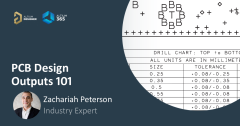
Holes & Slots
This is best shown with a Drill Table and produced with an NC Drill File. (Check hole sizes with Panels/PCB/Hole Size Editor.)
- Number of different hole sizes. These should be in increments of 2 mils (0.05mm) for consistent, cost effective results.
- Definitions for Plated, Non-Plated, and depth (Blind, Buried, and back drilled).
Figure 1. Drill drawing view
Number of PCB Layers and Layer Type
This includes a GERBER for each process layer – copper, gold plating (if present), soldermask, and silkscreen. (Setup should be done in the Layer Stack.)
- Show a Layer stack and define where the signal and plane layers are. Number the copper layers to prevent confusion. Name the Top & Bottom soldermask & silkscreen layers and any other additive process layers.
- Thickness and material can be generic or specific depending upon your needs.
- Some companies also show a view of each copper layer.
- This isn’t really necessary but can help to quickly identify the “positive or negative” nature of the GERBER file. Many programs will produce “PLANE” layers as either a “positive” or “negative” image.
- It can also be a quick reference for the designer or design team to be sure all expected features have been defined correctly in each layer.
Figure 2. Layer Stack
Figure 3. Gerber Views
Fabrication Test Point Locations
After defining features in the layout as a Fabrication Test Point, you can export these in the IPC-D-356a Netlist file. (Set up in Outjob/Fabrication Outputs.)
- Sometimes the fabricator will want to have a copy of the Schematic to verify some of the nets. Depends on what requirements are being asked of the fabricator to ensure electrical features such as differential pairs and continuity through net-ties.
Provide Notes For:
- Tolerancing, manufacturing processes, and IPC product classification (helps to define the tolerances).
- Plating requirements
- Registration
- Soldermask material & color
- Silkscreen material & color
- Any special coatings or finishes (Conformal coating materials, gold plating, HASL, etc)
Figure 4. Fabrication Notes
What the Assembler Needs to Know
All the information that the assembler needs to know are presented in an ASSEMBLY DRAWING and accompanied by a set of processing files. The ASSEMBLY DRAWING can be done using Draftsman® and the processing files can be set up in the Outjob. These can also be ZIPPED into one package for the Assembler.
Assembly View From Top, Bottom, and Side
- If there are variants of the assembly, they should be noted in the view(s). This is where you SHOW which components don’t get installed and which ones do.
- Also, a quick reference dimension of the overall size (X & Y) of the board and a dimension of the height of the tallest component(s) on each side of the board.
- This gives the assembler a good quick reference to the type of machinery they will need to produce your boards.
- A 3D view is nice, but not always necessary. A 3D view is to clarify assembly intent and facilitate good communication.
Figure 5. Assembly View
Figure 6. Assembly view from the side
-
Define the placement/alignment variables/tolerances for components that must interface with other mechanical features in the completed part (such as an instrumentation panel, switch or button interface, or light pipe).
-
Use the same origin used in the fabrication drawing to define these location tolerances.
-
Use GDT tolerancing methodologies for X, Y, & Z locations.
-
Use details to assist with alignment accuracy if needed.
Provide a Pick & Place File From the Layout
- This is a generated text document with origin locations of each component. It is used in the set-up of the assembly machinery. The file lists the component locations relative to the PCB origin.
- NOTE: All SM components are placed (and thus referenced for location) using the CENTER of the part, not an edge! This is due to the type of placement machinery used – a suction tube robotic arm. Many TH components (or heavy components) are placed using a “grabber” type of robotic arm. Their location reference may be “Pin 1” or may be “body center”. For headers & TH connectors, use “Pin 1”. When there is a mix of SM & TH in the same part, use the body center.
Provide a BOM With Approved 2nd & 3rd Sources
This can be included on the Assembly drawing or as a separate document. BOM output can be done from either the schematic or the layout. There are many ways to produce a BOM.
-
Don’t leave alternate components up to the Assembler. Many components look the same and are NOT. All alternate components should have the same FORM, FIT, and FUNCTION!!
Figure 7. Bill of Materials
Provide Notes For:
- Tolerancing, manufacturing processes, and IPC product classification (helps to define the tolerances).
- Special component programming requirements.
- Additional assembly procedures AFTER soldering.
Figure 8. Assembly Notes
Define Assembly Test Procedures
This also can be included on the Assembly drawing or as a separate document. Options can include:
- Include Functional test requirements as needed.
- Provide a test program file if needed.
- Define assembly test points.
- These should be located away from component soldering joints and outside of all component bodies.
- They should be on a grid if using “bed-of-nails” test procedures. Specify the grid used.
The issues we all face while doing the set-up for Fabrication and Assembly files and documents often lie in just a few places. Look at the workarounds vs “good practice” methods being used in your environment and consider what can be improved.
Have more questions? Call an expert at Altium or read more to gain a deeper understanding of sending a complete documentation package to PCB fabrication with Altium Designer®.
Related Resources
Related Technical Documentation
Table of Contents
- Fabricator Needs to Know the Following Details
- Holes & Slots
- Number of PCB Layers and Layer Type
- Fabrication Test Point Locations
- Provide Notes For:
- What the Assembler Needs to Know
- Assembly View From Top, Bottom, and Side
- Provide a Pick & Place File From the Layout
- Provide a BOM With Approved 2nd & 3rd Sources
- Provide Notes For:
- Define Assembly Test Procedures
Altium is transforming the electronics industry so thoroughly that our web pages need a minute to catch up. For a short time, some information on this page may be outdated.
We appreciate your patience. It will be worth the wait!
Learn More
Thank you, you are now subscribed to updates.