PCB Design Tools Enhanced with an Advanced Free Gerber File Editor

To successfully manufacture today’s challenging PCB designs, you need to be able to create the latest Gerber X2 file formats in your design tool’s free Gerber file editor online.
ALTIUM DESIGNER
Getting manufacturing output files out is a breeze with the right CAD software.
For over 30 years the printed circuit board design and manufacturing industries have relied on Gerber editor files to transfer PCB image information from design to manufacturing. This data is the standard used all over the world, but it has its limitations. To provide solutions for those limitations there are now new data formats such as Gerber X2. The problem though is that a lot of PCB design systems are not yet compatible with these formats.
To get the best results from your PCB manufacturer you need to be able to send them the most complete information possible, and that means having design software that is equipped with these new data formats. Fortunately, there is one PCB design system that can provide you with the best design tool available and can output data in the latest file formats. The answer you are looking for is Altium Designer.
What’s in a Gerber File Format?
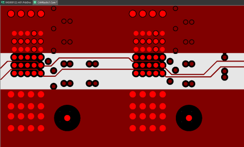
As the standard data format for building printed circuit boards, the Gerber PCB software file format has been in service for a long time. It communicates through a series of codes what shape should be flashed or drawn, and where those flashes and draws should be located in order to create an image. With the addition of aperture information at the top of each Gerber file, the extended Gerber or RS-274X format has been an excellent method of creating PCB editor images, but there are some limitations with it. It doesn’t have any way to identify which board layer is which without using a file naming convention, and there isn’t any other design data included except for the image information.
Individual Gerber editor files could be miss-named and switched around or missing altogether causing confusion for the PCB manufacturer. There also isn’t any accompanying netlist, layer stack, drill, or component information in the Gerber data. To transfer this data it must all be included in separate files and documented appropriately. To solve these problems the Gerber X2 data format was created. Now different layers can be identified, and full design data can be included.
Gerber File Data and Its Place in PCB Design
With a long history behind it, Gerber file maker data continues to grow and evolve as the design needs become more complex.
- The Gerber file is the past, present, and future.
- Gerber isn’t the only format used for manufacturing file outputs, here is some information on the other formats and how they compare.
Learn More about manufacturing file formats and what the future holds.
- See how Gerber files work into the entire PCB manufacturer design development process starting with schematic capture and going through PCB layout.
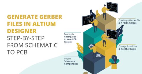
Learn More about the PCB design development process from schematic to final outputs.
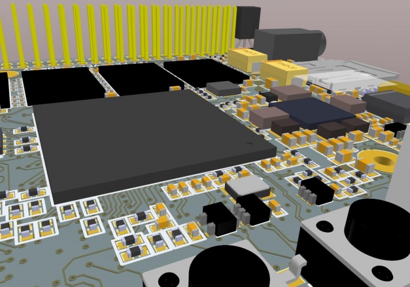
The latest Gerber X2 file formats are needed to successfully manufacture today’s PCB designs
Manufacturing Output Files in Altium Designer
To get your printed circuit board out of the design phase and into manufacturing, you need to create its manufacturing file formats. The Gerber files that you create are the start, but you also need other files such as a bill of materials, XY location files, and drawings. Altium Designer has you covered for all of this with Gerber and Gerber X2 file formats, as well as tools and utilities for all of the other files.
To create your manufacturing drawings, Altium Designer’s Draftsman is a powerful tool to do the heavy lifting of drawing generation for you. And when you have all of your outputs ready to go, there’s no need to worry about combining them all together. Altium Designer’s batch output job files can be configured to create the precise set of manufacturing files that you need.
Altium Designer has Everything you Need to Create Quality Output Files
Altium Designer gives you the features and functionality that you need to create all of your manufacturing output files.
- Altium Designer gives you many options for creating your Gerber files.
Learn More about Gerber file maker online in Altium Designer in this brief tutorial.
- You don’t need to be weighed down with creating your drawings anymore. Altium Designer’s Draftsman will auto-generate the drawings you need based on templates that you create.
Learn More about using Altium Designer’s Draftsman to create manufacturing drawings.
- When it’s time to put all of your manufacturing files together you can easily create them using Altium Designer’s user-configurable batch output job files.
Learn More about reusable batch output job files in Altium Designer.

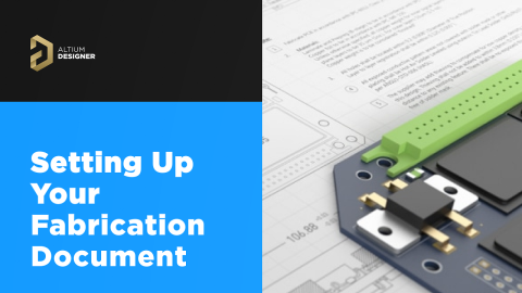
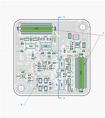
Manufacturing drawings like this can be easily created using Altium Designer’s Draftsman
Powerful PCB Design Software from Schematic to Layout
Altium Designer has all the options you need to create the exact set of manufacturing files that your PCB fabrications and assembly vendors will need. Before you are ready to create output files though, you need to design the board in the first place and Altium Designer has everything that you will need. Starting with the schematic, Altium Designer is your best choice with Gerber editor software that is easily learned and used and yet can handle the toughest design challenges like multi-channel design and hierarchy. In addition, you have tools to query part availability and price information directly from your preferred vendors as well as different simulators to work with.
In layout, Altium Designer is loaded with advanced functionality for footprint creation, part placement, and trace routing. You will have no trouble routing your designs to 100% completion with Altium Designer’s different routing tools. Manual interactive routing, differential pair routing, trace glossing, auto-interactive routing, and full-on auto routing are just some of the different features available to you. No matter the size, shape, or density of your PCB, Altium Designer has the power you need to complete your design successfully.
Altium Designer Gives You the PCB Design Tools You Need for Success
From Schematic capture to PCB layout, Altium Designer has been created with PCB designers in mind.
- Altium Designer’s schematic capture tools put the fun back into circuit creation.
Learn More about Altium Designer’s schematic capture application.
- With all of the different features and functions available to you, trace routing in Altium Designer will go swiftly and efficiently.
Learn More about interactive trace routing in Altium Designer.
- Altium Designer has been built from the ground up to provide all the PCB design tools you need in one suite of tools that all share a common interface to make your job easier.
Learn More about Altium Designer’s unified design environment.
You need the best PCB design tools with the latest file extensions & formats in its free Gerber file maker online to be successful with today’s challenging designs. Altium Designer has a Gerber editor ready for you to use in the most powerful and versatile set of PCB design tools that you can get.


