


Avoiding Costly Delays: Essential Tips for PCB Designers


Have you ever experienced the frustration of having your PCB design order placed on hold by your fabricator? This is a common issue that many PCB designers face, particularly with new flexible circuits or rigid-flex designs. When an order is placed, the anticipation of a smooth production process can be quickly disrupted by an unexpected hold, often due to engineering questions or clarifications. These holds are not just minor inconveniences—they can lead to significant delays in your project timeline, disrupting schedules, increasing costs, and straining relationships with clients or stakeholders.
Delays in PCB fabrication are often preventable and stem from issues in the submitted data package. Missing or incomplete information, inconsistencies, and overlooked details frequently disrupt production, leading to hold-ups. By identifying and addressing these common errors upfront, you can streamline your process and improve the success rate of your PCB projects.
Documentation: The Root of Many Delays
It is common for 60% or more of new designs to go "on hold" for clarification when the fabricator is setting up the tooling and process flow. This percentage can be even greater with flex and rigid-flex designs. The good news? Most of these problems are preventable. Before submitting your order, carefully review the entire documentation package and purchase order requirements. Double-check that everything is included and accurate.
Key Areas to Focus On
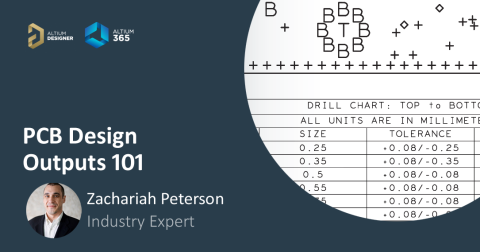
- Drill Charts: The drill chart outlines the specific sizes, quantities, and locations of the holes required in your PCB. A mismatch between the drill chart and the supplied drill files is one of the most common reasons for a project to be put on hold. This discrepancy indicates that the fabrication drawing and the actual design data may not be aligned, prompting the fabricator to stop the process to seek clarification. This can delay the CAM (Computer-Aided Manufacturing) process right from the start, extending your project timeline unnecessarily.
- Stack-Ups: The stack-up information details the arrangement of the various layers in your PCB, including the materials used and their respective thicknesses. Accurate stack-up data is essential for achieving the correct impedance and ensuring that the board performs as expected.
- Impedance Tables: Impedance control is crucial for high-speed circuits, and any errors in the impedance table can result in boards that don’t meet the required electrical performance. It’s important to verify that the specified impedance values are consistent with the actual design and that all necessary calculations are correct. Any discrepancy here could lead to a product that fails to meet your electrical specifications, necessitating rework or, worse, a complete redesign.
- PCB Dimensions: The overall dimensions of the PCB, including edge tolerances and critical feature locations, must be precisely documented. Any deviation between the drawing and the actual design data can cause significant issues during fabrication. For example, incorrect dimensions might result in the PCB not fitting properly into its intended enclosure or failing to align with other components, leading to costly modifications or scrapped boards.


Before submitting your fabrication drawing, thoroughly review all notes, dimensions, and details to ensure accuracy and alignment with the latest design revision. Confirm the dataset is complete, including circuit layers, drill files, solder masks, legends, netlists, array instructions, and drawings, and matches the correct revision. A common mistake—submitting outdated drill files while using updated circuit layers—can cause significant delays. By double-checking for consistency and completeness, you can avoid costly setbacks and streamline the fabrication process.
Example: Annular Ring and Drill-to-Copper Distance in NFPs
A common example where feature sizing can impact quality, cost, and delivery schedule is the annular ring size and drill-to-copper distance, specifically as they relate to non-functional pads (NFPs). Flexible materials are more challenging to work with than rigid ones, making it harder to maintain inner layer registration. Whenever possible, design larger annular rings into your flex layers to accommodate these challenges. For designs that require multiple lamination cycles, increasing the annular ring after the first cycle can enhance reliability.
Additionally, resist the temptation to remove nonfunctional pads when laying out traces. These pads act as a safe keep-back distance between a drill and a conductor. Removing them can compromise the reliability of your PCB and may violate IPC design guidelines.
Here’s an example of what can go wrong if you remove nonfunctional pads:
- Design spec: .008" drill-to-copper.
- Permitted tangency: .005" annular ring allows drill-to-copper to be .003" before etch-back.
- Etch back: Removes .0015", reducing the distance between copper plating and a conductor to .0015".
- CAF migration: Could add up to .001" growth, leaving just .0005" between them.
- IPC-2221/2222 requirements: A minimum of .002" space is needed for 0-50 volts in the finished product.
In a worst-case scenario, the plated hole could exceed its space budget by .0015". While this might be acceptable for class 2 products, it poses a significant risk for class 3 products and field reliability.
By paying close attention to your documentation, fabrication data set, and key design details like the annular ring and drill-to-copper distance, you can avoid unnecessary delays and ensure your PCB design meets all requirements. Taking these steps will not only save you time and frustration but will also lead to a more reliable final product.
About Author
Related Resources
Related Technical Documentation
Table of Contents
Design to Release, Without the Friction
- Keep reviews tied to the right version
- Reduce handoff confusion and rework
- Spot sourcing and release risk earlier
- Work solo, share when needed
Get Started
Thank you, you are now subscribed to updates.

