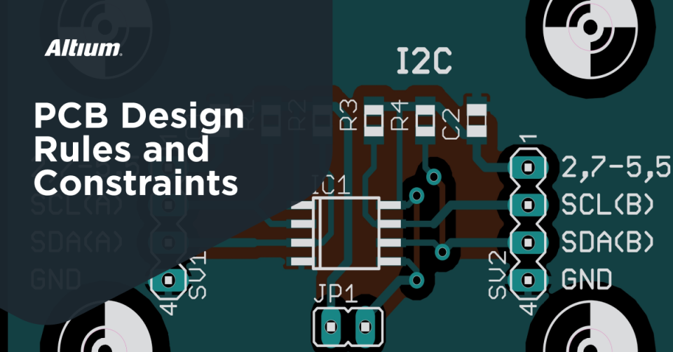
Well-defined design rules are the backbone of successful PCB layout. Explore how constraint-driven design ensures consistency between schematics and layout, prevents costly errors, and enables fast, automated workflows from concept to production.
ECAD software keeps designers honest by enforcing PCB design rules and constraints on the design and layout tools. It is
More layers and advanced via technology gives you more freedom to route as well as more stringent constraints on how you design your PCB stackup. See why in this article.
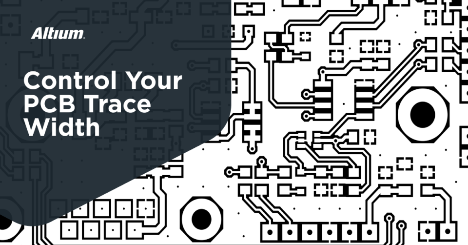
What seems like a simple selection of trace width is actually a critical engineering decision that relates to fabrication constraints and PCB stackup design.
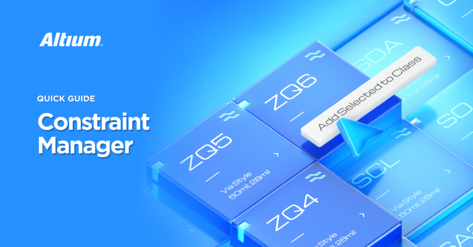
Learn all about Altium's New Constraint Manager with Andy Critcher, Director at Total Board Solutions, especially the revolutionary design constraint application for multiple nets. Whether tackling high-voltage designs, complex boards, or boosting productivity, this suite of tools promises to streamline workflows for the forward thinking PCB Designer.
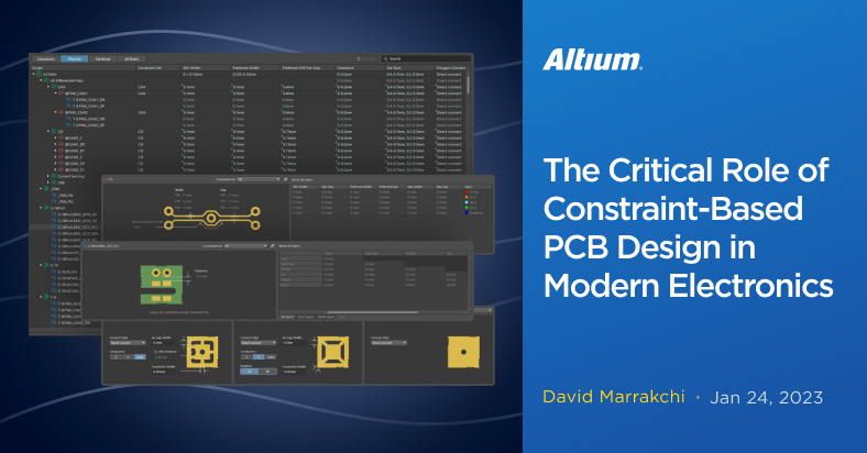
Welcome to the intricate realm of PCB (Printed Circuit Board) design, where what begins as a simple circuit board evolves
Simplify PCB design with Altium Designer’s Constraint Manager. Centralize rule management and boost efficiency. Download the whitepaper now.