







Design Constraints That Comes From the PCB Stackup

At a Glance
More layers and advanced via technology gives you more freedom to route as well as more stringent constraints on how you design your PCB stackup. See why in this article.


Your PCB stackup defines much more than the number of copper layers in the board. It establishes the physical limits that control via geometry, trace width, spacing, routing density, impedance, copper thickness, and fabrication sequence. Most importantly, simply adding layers or blind/buried vias does not give you unlimited routing freedom, instead it changes the constraints in the design and can restrict your ability to route, assemble, and/or fabricate the design.
Fortunately, understanding these factors can help designers make smarter stackup decisions rather than relying on higher layer counts and advanced via stacks as crutches. The worst case is completing a design, only to find that it can not be manufactured given the constraints used to complete the layout. Designers can avoid these problems by understanding how the PCB stackup drives specific design rules in the PCB layout.
How Your PCB Stackup Drives Design Rules
As component count and interconnect density increase, PCB layer count usually increases as well. This is generally done to accommodate modern BGAs and fine-pitch bottom-terminated packages, causing the layer count and total stackup thickness to grow in response. High-speed interfaces may also require specific dielectric thicknesses to achieve controlled impedance with manufacturable trace widths.
These requirements interact with total board thickness. A high layer count board built from relatively thick dielectric layers can quickly become too thick for standard through-hole drilling. Very thin dielectric layers can improve routing density, but they can also push the design toward HDI fabrication processes. The stackup therefore has to balance routing density, impedance requirements, total thickness, and fabrication capability.
The most common stackup-driven constraints can be summarized as follows:
Feature | Primary constraint | Design consequence |
Through-hole vias | Board thickness versus drill diameter | Small drills in thick boards can exceed allowable aspect ratio |
Blind and buried vias | Via depth versus drill diameter | Deep spans may require separate sub-laminations |
Copper routing | Finished copper weight | Heavier copper requires larger trace widths and clearances |
Microvias | Dielectric thickness and via diameter | Thin buildup layers are required for reliable laser drilling |
Through-Hole Via Aspect Ratio
Through-hole vias are one of the easiest places to create an unmanufacturable design. The governing value is the aspect ratio between board thickness and finished hole diameter. As the board becomes thicker or the drill becomes smaller, plating the full depth of the via becomes more difficult. However, for multiple reasons, PCB design software does not allow users to define aspect ratio as a design rule, and instead requires the user to define minimum allowed hole sizes for different via types.
For example, placing 0.15 mm finished vias into a 2 mm thick PCB creates a very aggressive aspect ratio that most fabrication houses will reject. Even on a nominal 62 mil (1.57 mm) board thickness, that drill size may be outside the standard process capability of many fabricators. This becomes especially relevant when large BGAs or dense QFN layouts encourage designers to reduce via diameter to create more routing channels:
- In a large BGA that can take through-holes in fanout routing, more pins equates to more layers in the stackup, and thus larger thickness
- As you increase the board thickness, through-holes will get closer to the aspect ratio limit, and making them larger eventually hits the clearance limit
The correct constraint should come from the fabricator rather than from a generic PCB design rule. Most fabrication houses will accept an 8 mil drill diameter in a standard thickness PCB manufactured to IPC Class 2 workmanship standards; for Class 3, they may reduce the allowed aspect ratio. Once the maximum supported aspect ratio is known, the minimum allowable drill diameter can be determined from the intended board thickness.
Copper Weight Changes Routing Rules
Copper weight is another stackup parameter that constrains routing density. As finished copper gets thicker, the minimum manufacturable trace width and copper-to-copper spacing generally increase. In terms of PCB design rules, this means inner and outer layers may require different routing constraints. A common stackup might use 0.5 oz copper on internal layers and 1 oz finished copper on the outer layers. The outer layers would then require much larger minimum widths and clearances than the internal routing layers.
The distinction between base copper and finished copper also matters. Outer layers gain additional copper during through-hole plating, so a layer that begins as 1 oz. copper foil might finish much thicker. Designers should therefore specify finished copper requirements in fabrication documentation and use design rules that reflect the finished copper weight.
Example clearance/feature size minima vs. copper weight (note: a different table would be used for internal layers)
Copper Weight | Nominal Foil Thickness | Standard Min. Feature Size (Trace Width) | Standard Min. Clearance (Spacing) | Advanced Min. Feature Size (Trace Width) | Advanced Min. Clearance (Spacing) |
0.5 oz. | 0.7 mil (17.5 µm) | 4 mil (0.10 mm) | 4 mil (0.10 mm) | 3 mil (0.076 mm) | 3 mil (0.076 mm) |
1.0 oz. | 1.37 mil (35 µm) | 5 mil (0.127 mm) | 5 mil (0.127 mm) | 4 mil (0.10 mm) | 4 mil (0.10 mm) |
2.0 oz. | 2.74 mil (70 µm) | 8 mil (0.203 mm) | 8 mil (0.203 mm) | 6 mil (0.15 mm) | 6 mil (0.15 mm) |
Source references: Bittele Electronics and PCBWay.
Once copper thickness reaches 2 oz or more, trace spacing, etch tolerance, resin fill, solder mask coverage, and solderability all become more restrictive. This is why, in many power electronics designs, or digital designs that also require high currents, adding additional 1 oz routing or plane layers can provide much more design freedom than forcing heavy copper films onto a small number of layers. In terms of the cost, the two approaches are basically the same.
Blind and Buried Vias in Sub-laminations
Mechanically drilled blind and buried vias introduce constraints that are tied directly to the fabrication sequence and standard fabrication capabilities, particularly regarding drilling. There are important rules regarding blind/buried vias in sub-laminations:
- Start and end rule - A mechanically drilled blind/buried via span may not end on the same layer as the start of a different mechanically drilled via span. The exception is if sequential lamination is used, or you will need laser-drilled blind vias, which would allow stacking.
- No crossing vias - Mechanically drilled blind/buried via spans may not cross over each other, but the via spans can be nested.
- Prepreg bonding - When bonding sub-laminations, the sub-stacks can only be bonded together with prepregs, not with cores.
As a basic design approach, if you are targeting a specific buried via diameter (such as for BGA fanout), then the drill aspect ratio must be planned while creating the stackup. Each unrelated blind/buried via span can require additional sub-laminations, drilling operations, and plating steps, each of which adds copper weight, increases clearance/size requirements, and reduces the allowed aspect ratio.
The plating process also changes the copper thickness at the beginning and end of mechanically drilled buried via spans. Those exposed copper layers receive additional plating when the buried via barrels are formed. The resulting finished copper thickness can affect routing clearances, impedance calculations, and etch compensation on those layers.
Sequential Lamination and HDI Constraints
Sequential lamination introduces another set of limits when laser-drilled microvias are used. The allowed laser drilling diameter depends on the dielectric thickness between adjacent copper layers and aspect ratio of <1 is normally required, which is why HDI buildup layers are typically thin. If the dielectric becomes too thick relative to the laser-drilled diameter, the via exceeds the fabricator's supported microvia aspect ratio.
Each sequential buildup cycle also adds fabrication steps. Stacked microvias may require filled and planarized vias before another microvia can be placed directly above them, and fabricators may limit the number of stacked levels they will support. Staggered microvias can avoid some of these stacking requirements, but they consume more routing area.
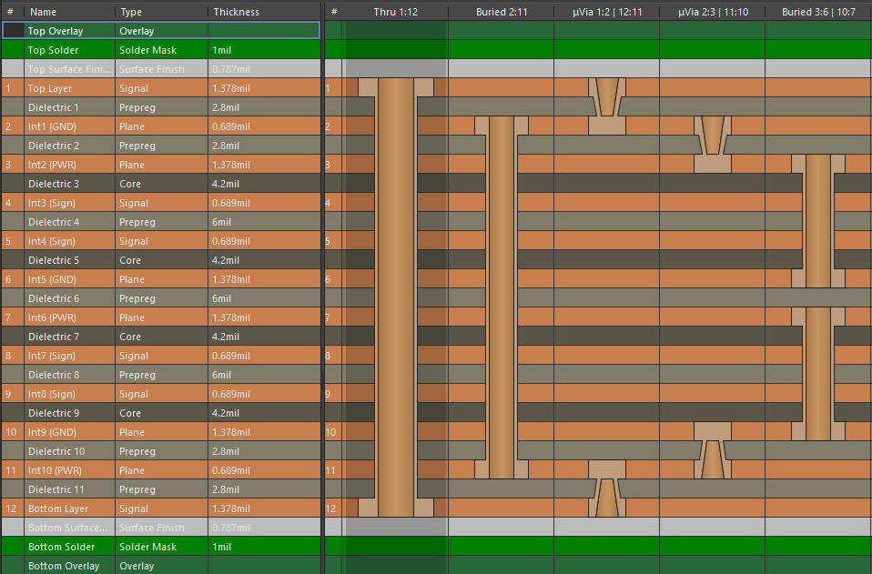
Many practical HDI stackups combine sequential lamination with a mechanically drilled buried-via core. This gives the designer both microvias near the outer layers and longer buried connections through the center of the board. A common option that supports microvia stacking into inner layers and overlapping BGAs on both sides of the PCB is shown below.
Define Fabrication Constraints Before Routing
The most efficient PCB stackup is one that supports the required routing without pushing fabrication into unnecessary process steps. Before placement and routing begin, use the finished copper weights, allowable mechanical drilling aspect ratio, and any microvia stacking from the selected fabricator to define a few basic design rules:
- Copper feature size and space
- Vias size limits for various via types
- Trace width/spacing values for controlled impedance lines
- Define copper features for both inner and outer layers and based on copper weight
Those simple PCB design rules prevent the layout from drifting into something requiring extensive redesigns to become manufacturable. To better understand the design rules and limitations imposed by buried via structures in more advanced stackups, watch the video below.
Whether you need to build reliable power electronics or advanced digital systems, use Altium’s complete set of PCB design features and world-class CAD tools. Altium provides the world’s premier electronic product development platform, complete with the industry’s best PCB design tools and cross-disciplinary collaboration features for advanced design teams. Contact an expert at Altium today!
Frequently Asked Questions
How does PCB thickness affect through-hole via aspect ratio?
PCB thickness directly affects the aspect ratio of a through-hole via. As the board becomes thicker, a given drill diameter produces a higher aspect ratio, which makes uniform barrel plating more difficult. Designers should determine the fabricator’s maximum supported aspect ratio and use the intended board thickness to establish the minimum allowable finished hole diameter.
When does a PCB stackup require sequential lamination?
Sequential lamination is typically required when the stackup uses laser-drilled microvias that connect multiple buildup layers or when via structures cannot be produced in a single conventional lamination cycle. Each buildup cycle adds fabrication steps, and stacked microvias may need to be filled and planarized before another microvia can be placed above them.
Can blind and buried vias cross or overlap in a PCB stackup?
Mechanically drilled blind and buried via spans generally cannot cross each other, although they can be nested. One mechanically drilled via span also cannot terminate on the same layer where another mechanically drilled span begins unless sequential lamination is used. Laser-drilled microvias provide additional flexibility and can support stacked structures when the fabrication process allows them.
Why do outer PCB layers require different trace and spacing rules than inner layers?
Outer PCB layers can require larger trace widths and clearances because they receive additional copper during through-hole plating. As a result, their finished copper thickness can be greater than the starting foil thickness and greater than the copper used on internal layers. PCB design rules should therefore reflect the finished copper weight of each layer rather than applying identical rules across the entire stackup.
How does copper weight affect PCB trace width and spacing?
As finished copper weight increases, the minimum manufacturable trace width and copper-to-copper spacing generally increase. Heavier copper requires more allowance for etching and fabrication tolerances, reducing the routing density available on that layer. For example, the article shows standard minimum feature sizes increasing from 4 mil at 0.5 oz copper to 8 mil at 2 oz copper.

About Author
Related Resources
Related Technical Documentation
Table of Contents
- How Your PCB Stackup Drives Design Rules
- Through-Hole Via Aspect Ratio
- Copper Weight Changes Routing Rules
- Blind and Buried Vias in Sub-laminations
- Sequential Lamination and HDI Constraints
- Define Fabrication Constraints Before Routing
- Frequently Asked Questions
- How does PCB thickness affect through-hole via aspect ratio?
- When does a PCB stackup require sequential lamination?
- Can blind and buried vias cross or overlap in a PCB stackup?
- Why do outer PCB layers require different trace and spacing rules than inner layers?
- How does copper weight affect PCB trace width and spacing?
Solutions for Every Role and Team
- Discover and evaluate design options earlier
- Develop in one shared workspace
- Scale with control and compliance
- Connect every stage of hardware development
Learn More
Thank you, you are now subscribed to updates.



