


The Best PCB Design Rules System Keeps Your Board Error Free


ECAD software keeps designers honest by enforcing PCB design rules and constraints on the design and layout tools. It is the PCB designer's responsibility to create design rules for any new design, with the end goal being to ensure functionality and manufacturability. Over time, the major ECAD software vendors have developed two formats for defining PCB design rules: a category-based entry system and a matrix-based system for defining constraints.
Either format is acceptable and can produce the exact same results, with the selection of category-based or constraint-based design rule definitions coming down to personal preference. No matter which of these mechanisms you choose to use, select the PCB design software package that gives you the flexibility you need to fully control your PCB design rule definitions.
Where Do PCB Design Rules Come From?
What are the factors that drive PCB design rules and why do these matter? PCB design rules are defined based on a few possible requirements:
- Manufacturability constraints
- Assembly constraints
- Signal integrity requirements
- EMI/EMC requirements
- Defined as an enabler for RF design
This is just a cross-section of the areas where design rules are spawned. Note that PCB design rules are not based on simple electrical functionality. Instead, most PCB design rules and constraints are defined based on manufacturing requirements. If a board cannot be manufactured, then there is no point in designing it, thus design for manufacturing (DFM) rules are some of the most basic PCB design rules in industry technical content.
PCB Design Rules Versus Constraints
Some PCB design software will use the term "rules" while other software will use the term "constraints." The reality is that there is very little difference between a design rule and a design constraint; the difference between these is simply the vocabulary that different software vendors choose to use. The two terms are used specifically in reference to the user interface for creating PCB design rules in ECAD software.
With this in mind, PCB design software vendors tend to make the distinction between a rule and a constraint as follows:
- A design rule is typically defined within a category-based system, where individual rules are organized under hierarchical categories (such as Routing, Manufacturing, Electrical, and Placement). Each rule is configured with scope definitions that determine which objects or nets the rule applies to, and values are entered through dedicated configuration dialogs. Rules can be prioritized so that more specific rules override general defaults.
- A design constraint is typically defined within a matrix-based or tabular system, where values are entered directly into cells at the intersection of net classes, layers, or object types. This approach presents all constraint values in a single spreadsheet-like view, making it straightforward to compare values across multiple nets or classes simultaneously.
In practice, both approaches enforce the same geometric and electrical checks during design rule checking (DRC). The distinction is purely one of workflow preference: category-based rules offer granular scoping and prioritization logic, while matrix-based constraints offer rapid visual comparison and bulk editing across the design.
Altium Designer is unique in that it is the only PCB design software platform that allows users to fully specify their design and manufacture requirements as either design rules or design constraints. The primary method uses the category-based PCB Rules and Constraints Editor, where all supported design rule categories are listed hierarchically. Each rule is configured individually with a scope definition that determines which objects, nets, or net classes the rule applies to.
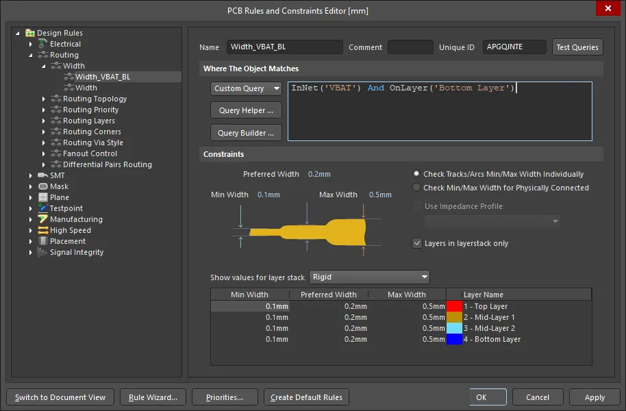
PCB Rules and Constraints Editor in Altium Designer
Altium Designer also provides a constraint manager that uses a matrix-based approach for specifying design requirements. This interface presents all design constraints in a tabular spreadsheet format that will be immediately familiar to users of other ECAD software platforms, including legacy platforms like Cadence Allegro and Mentor Graphics. The matrix view allows designers to see all constraint values simultaneously, compare settings across net classes at a glance, and make bulk edits without navigating through individual rule dialogs.
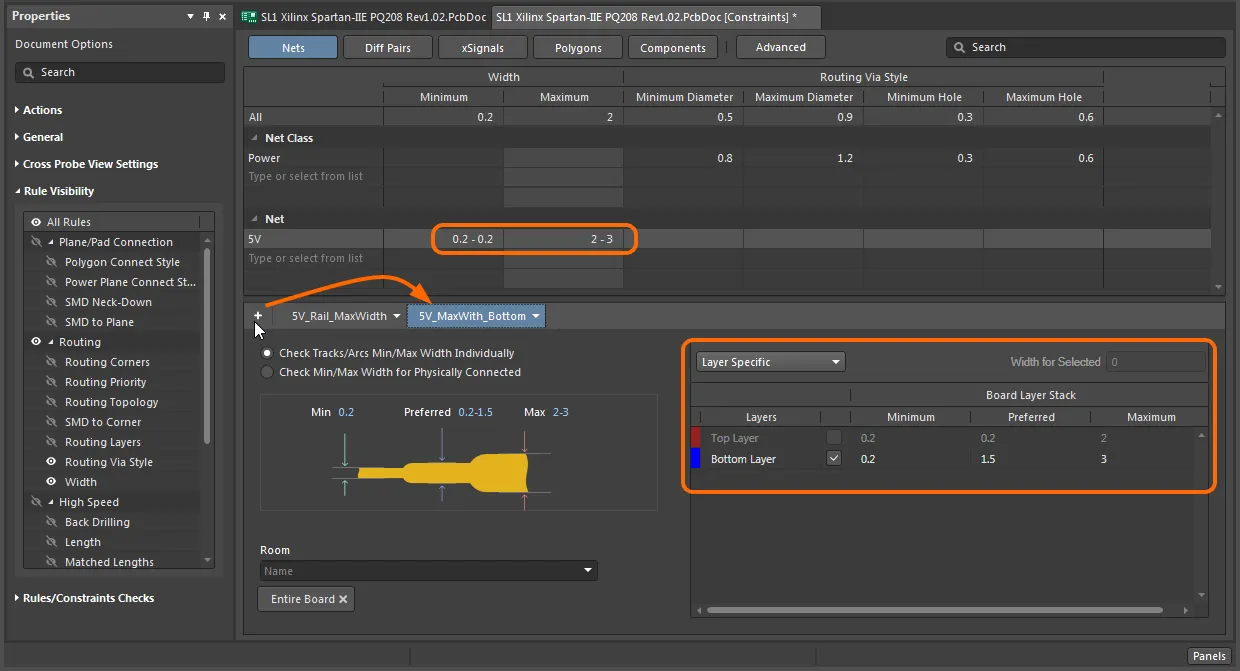
Constraint Manager in Altium Designer
With either approach, designers gain full control over the specifications of their design, and this will help prevent many of the simpler problems that can lead to defects in manufacturing. To access the major design rules in either approach, the table below provides useful reference instructions and access details. Follow these instructions or read the Altium Documentation to learn more.
DFM Requirement | Rules-Based Approach | Constraint-Based Approach |
Minimum trace width | Defined under the Routing > Width rule category with scope set per net class; min, preferred, and max values entered in a configuration dialog | Entered as a numerical value in the width column at the intersection of the relevant net class row |
Copper-to-copper clearance | Defined under the Electrical > Clearance rule category with separate rules scoped to net classes or object pairs, prioritized by specificity | Entered directly in clearance matrix cells at the intersection of each net class pair |
Minimum drill hole size | Defined under the Manufacturing > Hole Size rule category with min and max values specified per via or pad type | Entered as min/max values in the drill size row for each via class or component group |
Annular ring minimum | Defined under the Manufacturing > Minimum Annular Ring rule with scope applied globally or per pad class | Entered as a single numerical value in the annular ring column, applied per via or pad class |
Solder mask expansion | Defined under the Manufacturing > Solder Mask Expansion rule with scope set per component class or pad type | Entered as an expansion value in the solder mask column for each pad or component class |
Board edge clearance | Defined under the Manufacturing > Board Outline Clearance rule with a single global scope or per-object scoping | Entered as a clearance value in the board edge row applied uniformly or per object type |
Types and Categories of PCB Design Rules
The major design rules for any new design can be determined based on the product specification and capabilities of the circuit board manufacturer. Some design rule values may need to be calculated by hand, which is based on several possible factors:
- Recommendations or performance goals in certain industry standards
- Directly from the PCB fabrication house capability statements
- Mechanical constraints such as from a device enclosure
- Signal integrity constraints, such as impedance or trace-to-trace spacing
- Power integrity requirements such as from minimum copper rail size calculations
Simple design rule values can be entered numerically, especially in the case of a constraint management approach with a numerical matrix. The most common of these are clearance values between copper features, components, mechanical elements, drilled holes, slots, and the PCB edge.
The table below offers a summary of the most common PCB design rules that apply to almost every project. These rules span across multiple categories (routing, manufacturability, etc.) and they form a useful checklist for rules definition in a new project.
Design Rule Category | Specific Rule Name | Basis for Value |
Routing | Width | Calculated from current-carrying requirements or specified by impedance targets for controlled-impedance nets |
Routing | Impedance | Calculated from stackup geometry, dielectric constant, and target characteristic impedance using field-solver tools |
Routing | Differential Pair Routing | Calculated from differential impedance targets, coupling geometry, and dielectric properties |
Electrical | Clearance | Specified by fabrication house minimum copper-to-copper spacing or calculated from voltage isolation requirements |
Manufacturing | Specified directly from fabrication house capability statements based on drill registration tolerance | |
Manufacturing | Hole Size | Specified by fabrication house minimum drill diameter or calculated from via current-carrying needs |
Manufacturing | Solder Mask Expansion | Specified by fabrication house registration tolerance for solder mask layers |
Manufacturing | Board Outline Clearance | Specified by fabrication house routing tolerance or mechanical enclosure constraints |
High Speed | Matched Net Lengths | Calculated from timing budgets and propagation delay requirements for synchronous interfaces |
High Speed | Max Via Count | Determined from signal integrity simulation or loss budgets for high-frequency channels |
Placement | Component Clearance | Specified by assembly house minimum pick-and-place tolerances or mechanical enclosure constraints |
PCB Design Rule Checks (DRCs)
PCB design rule checks are run automatically (online) and as groups (batch) to ensure that the features in a PCB comply with your design rules and constraints. Online checks will flag errors as you create the PCB layout, while batch checks are run against all the relevant design rules in the PCB.
Once violations are reported, the designer will have to prioritize some of these violations for correction, leading to changes in the PCB layout. The goal in any design is to get down to zero DRC violations, and this often requires some amount of changes to the PCB layout after running the initial DRC.
The process of reducing DRC violations to zero involves carefully updating the PCB layout to clear those errors, often making many minor adjustments to the design until the errors are resolved. Most often, these errors involve slight positional changes to various objects in the PCB layout, or possibly some trace re-routing or polygon drawing updates. At the end of this process, the designer produces a completely cleaned PCB layout that aligns with the constraints defined at the beginning of the project.
Does Zero DRCs = Zero Defects?
The answer to this question is a definite “no.”
This is because there are many defect causes that are beyond the designer’s control or that are not impacted by the PCB layout. For example, stackup design and processing can impact fabrication defects in certain designs, despite the fact that the PCB layout contains zero DRCs. Ensuring a design is defect-free goes well beyond the PCB layout and requires a holistic understanding of PCB design, ranging from stackup to specifying master drawings for manufacturing.
To learn more about some common causes of defects beyond the PCB layout, watch the video below. See if you can spot which of these problems can be influenced by choices in the PCB layout and defining design rules/constraints in your ECAD software.
Whether you need to build reliable power electronics or advanced digital systems, use Altium’s complete set of PCB design features and world-class CAD tools. Altium provides the world’s premier electronic product development platform, complete with the industry’s best PCB design tools and cross-disciplinary collaboration features for advanced design teams. Contact an expert at Altium today!
Frequently Asked Questions
Where do PCB design rules come from in a new PCB project?
PCB design rules come from fabrication limits, assembly requirements, SI/PI targets, EMI/EMC needs, RF constraints, and mechanical requirements. Many basic rules, such as trace width, clearance, drill size, annular ring, and solder mask expansion, come directly from the fabricator’s capabilities.
What is the difference between PCB design rules and PCB design constraints?
The difference is mostly workflow. Rules are usually configured in category-based editors, while constraints are usually entered in tables or matrices. Both can enforce the same layout requirements during DRC.
Are category-based design rules better than matrix-based constraints?
No. Category-based rules are better for detailed scoping and priorities, while matrix-based constraints are better for comparison and bulk editing. The best choice depends on the design and the designer’s workflow.
What does a PCB design rule check actually verify?
DRC verifies whether the layout follows the defined rules and constraints. It can flag clearance, width, hole size, annular ring, solder mask, component spacing, and high-speed routing violations.
Does passing DRC mean a PCB will have zero manufacturing defects?
No. Passing DRC only means the layout follows the rules that were defined. Defects can still come from stackup choices, fabrication variation, weak documentation, assembly issues, or incorrect rule values.

About Author
Related Resources
Related Technical Documentation
Table of Contents
Design to Release, Without the Friction
- Keep reviews tied to the right version
- Reduce handoff confusion and rework
- Spot sourcing and release risk earlier
- Work solo, share when needed
Get Started
Thank you, you are now subscribed to updates.


